- 您現在的位置:買賣IC網 > PDF目錄373923 > AD7890BR-10 (ANALOG DEVICES INC) LC2MOS 8-Channel, 12-Bit Serial, Data Acquisition System PDF資料下載
參數資料
| 型號: | AD7890BR-10 |
| 廠商: | ANALOG DEVICES INC |
| 元件分類: | ADC |
| 英文描述: | LC2MOS 8-Channel, 12-Bit Serial, Data Acquisition System |
| 中文描述: | 8-CH 12-BIT PROPRIETARY METHOD ADC, SERIAL ACCESS, PDSO24 |
| 封裝: | MS-013AD, SOIC-24 |
| 文件頁數: | 13/20頁 |
| 文件大小: | 302K |
| 代理商: | AD7890BR-10 |
AD7890
–13–
REV. A
T he duration of the internal pulse can be seen on the C
EX T
pin.
T he C
EX T
pin goes from a low to a high when a serial write to
the part is initiated (on the falling edge of
TFS
). It starts to
discharge on the sixth falling edge of SCLK in the serial write
operation. Once the C
EX T
pin has discharged to crossing its
nominal trigger point of 2.5 V, the internal pulse is timed out.
T he internal pulse is initiated each time a write operation to the
Control Register takes place. As a result, the pulse is initiated
and the conversion process delayed for all software conversion
start commands. For hardware conversion start, it is possible to
separate the conversion start command from the internal pulse.
If the multiplexer output (MUX OUT ) is connected directly to
the track/hold input (SHA IN), then no external settling has to
be taken into account by the internal pulse width. In applica-
tions where the multiplexer is switched and conversion is not
initiated until more than 2
μ
s after the channel is changed (as is
possible with a hardware conversion start), the user does not
have to worry about connecting any capacitance to the C
EX T
pin. T he 2
μ
s equates to the track/hold acquisition time of the
AD7890. In applications where the multiplexer is switched and
conversion is initiated at the same time (such as with a software
conversion start), a 120 pF capacitor should be connected to
C
EX T
to allow for the acquisition time of the track/hold before
conversion is initiated.
If external circuitry is connected between MUX OUT and SHA
IN, then the extra settling time introduced by this circuitry will
have to be taken into account. In the case where the multiplexer
change command and the conversion start command are sepa-
rated, they need to be separated by greater than the acquisition
time of the AD7890 plus the settling time of the external cir-
cuitry if the user does not have to worry about the C
EX T
capaci-
tance. In applications where the multiplexer is switched and
conversion is initiated at the same time (such as with a software
conversion start), the capacitor on C
EX T
needs to allow for the
acquisition time of the track/hold plus the settling-time of the
external circuitry before conversion is initiated.
SE RIAL INT E RFACE
T he AD7890’s serial communications port provides a flexible
arrangement to allow easy interfacing to industry-standard
microprocessors, microcontrollers and digital signal processors.
A serial read to the AD7890 accesses data from the output reg-
ister via the DAT A OUT line. A serial write to the AD7890
writes data to the Control Register via the DAT A IN line.
T wo different modes of operation are available, optimized for
different types of interface where the AD7890 can act either as
master in the system (it provides the serial clock and data fram-
ing signal) or acts as slave (an external serial clock and framing
signal can be provided to the AD7890). T hese two modes,
labelled Self-Clocking Mode and External Clocking Mode, are
discussed in detail in the following sections.
Self-Clocking Mode
T he AD7890 is configured for its Self-Clocking Mode by tying
the SMODE pin of the device to a logic low. In this mode, the
AD7890 provides the serial clock signal and the serial data
framing signal used for the transfer of data from the AD7890.
T his Self-Clocking Mode can be used with processors which
allow an external device to clock their serial port including most
digital signal processors.
Read Operation
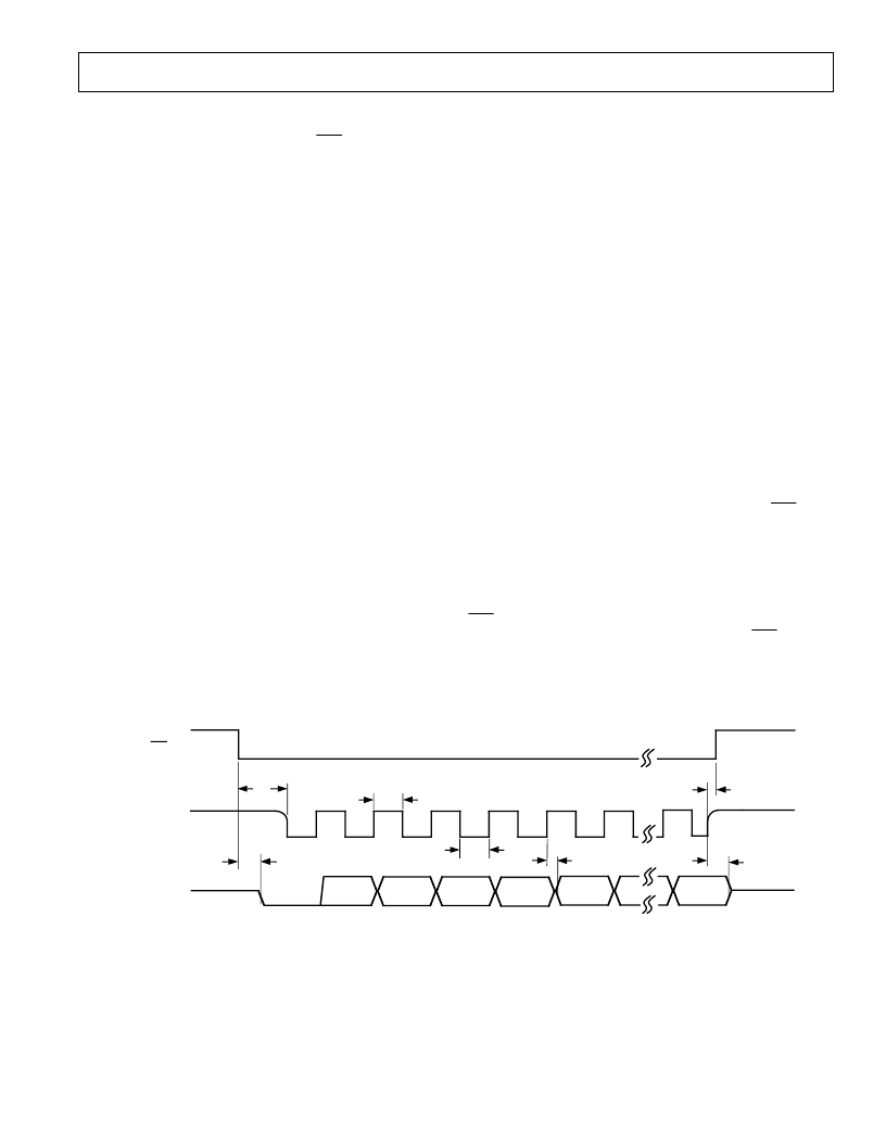
Figure 8 shows a timing diagram for reading from the AD7890
in the Self-Clocking mode. At the end of conversion,
RFS
goes
low and the serial clock (SCLK ) and serial data (DAT A OUT )
outputs become active. Sixteen bits of data are transmitted with
one leading zero, followed by the three address bits of the Con-
trol Register, followed by the 12-bit conversion result starting
with the MSB. Serial data is clocked out of the device on the ris-
ing edge of SCLK and is valid on the falling edge of SCLK . T he
RFS
output remains low for the duration of the sixteen clock
cycles. On the sixteenth rising edge of SCLK , the
RFS
output is
driven high and DAT A OUT is disabled.
SCLK (O)
DATA OUT (O)
RFS (O)
3-STATE
3-STATE
LEADING
ZERO
DB10
DB0
DB11
A0
A1
A2
t
2
t
3
t
5
t
4
t
6
t
7
t
1
NOTE
(I) SIGNIFIES AN INPUT; (O) SIGNIFIES AN OUTPUT. PULL-UP RESISTOR ON SCLK.
Figure 8. Self-Clocking (Master) Mode Output Register Read
相關PDF資料 |
PDF描述 |
|---|---|
| AD7890BR-2 | LC2MOS 8-Channel, 12-Bit Serial, Data Acquisition System |
| AD7890BR-4 | LC2MOS 8-Channel, 12-Bit Serial, Data Acquisition System |
| AD7890AR-10 | Side Entry Connector Hood; Enclosure Material:Aluminum Alloy; For Use With:C146 Rectangular Circular Connectors; Connecting Termination:Screw; Gender:Male; No. of Contacts:48; Operating Voltage:400V; Series:C-146 RoHS Compliant: Yes |
| AD7890AR-2 | Circular Connector Cable Assembly; Connector Type A:Circular Receptacle; Connector Type B:Stripped End Leads; Cable Length:10ft; Features:500 Mating Cycles, PVC Jacket, IP67 Rating, E63093 Rated Connector; No. of Contacts:6 RoHS Compliant: Yes |
| AD7890SQ-10 | 20 Characters x 4 Lines, 5x7 Dot Matrix Character and Cursor |
相關代理商/技術參數 |
參數描述 |
|---|---|
| AD7890BR-10REEL | 功能描述:IC DAS 12BIT 8CH 24-SOIC RoHS:否 類別:集成電路 (IC) >> 數據采集 - ADCs/DAC - 專用型 系列:- 產品培訓模塊:Lead (SnPb) Finish for COTS Obsolescence Mitigation Program 標準包裝:50 系列:- 類型:數據采集系統(DAS) 分辨率(位):16 b 采樣率(每秒):21.94k 數據接口:MICROWIRE?,QSPI?,串行,SPI? 電壓電源:模擬和數字 電源電壓:1.8 V ~ 3.6 V 工作溫度:-40°C ~ 85°C 安裝類型:表面貼裝 封裝/外殼:40-WFQFN 裸露焊盤 供應商設備封裝:40-TQFN-EP(6x6) 包裝:托盤 |
| AD7890BR-2 | 制造商:Analog Devices 功能描述:ADC Single SAR 117ksps 12-bit Serial 24-Pin SOIC W 制造商:Rochester Electronics LLC 功能描述:8-CH,100K,12-BIT ADC - Bulk |
| AD7890BR-2REEL | 制造商:Analog Devices 功能描述:ADC Single SAR 117ksps 12-bit Serial 24-Pin SOIC W T/R |
| AD7890BR-4 | 功能描述:IC DAS 12BIT 8CH 24-SOIC RoHS:否 類別:集成電路 (IC) >> 數據采集 - ADCs/DAC - 專用型 系列:- 產品培訓模塊:Lead (SnPb) Finish for COTS Obsolescence Mitigation Program 標準包裝:50 系列:- 類型:數據采集系統(DAS) 分辨率(位):16 b 采樣率(每秒):21.94k 數據接口:MICROWIRE?,QSPI?,串行,SPI? 電壓電源:模擬和數字 電源電壓:1.8 V ~ 3.6 V 工作溫度:-40°C ~ 85°C 安裝類型:表面貼裝 封裝/外殼:40-WFQFN 裸露焊盤 供應商設備封裝:40-TQFN-EP(6x6) 包裝:托盤 |
| AD7890BR-4REEL | 制造商:Analog Devices 功能描述:ADC Single SAR 117ksps 12-bit Serial 24-Pin SOIC W T/R 制造商:Analog Devices 功能描述:ADC SGL SAR 117KSPS 12-BIT SERL 24SOIC W - Tape and Reel |
發布緊急采購,3分鐘左右您將得到回復。