- 您現在的位置:買賣IC網 > PDF目錄373923 > AD7890SQ-4 (ANALOG DEVICES INC) 20 Characters x 4 Lines, 5x7 Dot Matrix Character and Cursor PDF資料下載
參數資料
| 型號: | AD7890SQ-4 |
| 廠商: | ANALOG DEVICES INC |
| 元件分類: | ADC |
| 英文描述: | 20 Characters x 4 Lines, 5x7 Dot Matrix Character and Cursor |
| 中文描述: | 8-CH 12-BIT PROPRIETARY METHOD ADC, SERIAL ACCESS, CDIP24 |
| 封裝: | 0.300 INCH, CERDIP-24 |
| 文件頁數: | 16/20頁 |
| 文件大小: | 302K |
| 代理商: | AD7890SQ-4 |
AD7890
–16–
REV. A
AD7890–68HC11 Interface
An interface circuit between the AD7890 and the 68HC11
microcontroller is shown in Figure 13. For the interface shown,
the AD7890 is configured for its external clocking mode while
the 68HC11’s SPI port is used and the 68HC11 is configured in
its single-chip mode. T he 68HC11 is configured in the master
mode with its CPOL bit set to a logic zero and its CPHA bit set
to a logic one.
As with the previous interface, there are no provisions for moni-
toring when conversion is complete on the AD7890. T o monitor
the conversion time on the AD7890 a scheme, such as outlined
in the previous interface with
CONVST
, can be used. T his can
be implemented in two ways. One is to connect the
CONVST
line to another parallel port bit which is configured as an input.
T his port bit can then be polled to determine when conversion
is complete. An alternative is to use an interrupt driven system
in which case the
CONVST
line should be connected to the
IRQ
input of the 68HC11.
SMODE
TFS
DATA OUT
DATA IN
SCLK
AD7890
RFS
PC0
PC1
SCK
68HC11
DV
DD
DV
DD
MISO
MOSI
SS
Figure 13. AD7890 to 68HC11 Interface
T he serial clock rate from the 68HC11 is limited to significantly
less than the allowable input serial clock frequency with which
the AD7890 can operate. As a result, the time to read data from
the part will actually be longer than the conversion time of the
part. T his means that the AD7890 cannot run at its maximum
throughput rate when used with the 68HC11.
AD7890–ADSP-2101 Interface
An interface circuit between the AD7890 and the ADSP-2101
DSP processor is shown in Figure 14. T he AD7890 is config-
ured for its external clocking mode with the ADSP-2101 provid-
ing the serial clock and frame synchronization signals. T he
RFS1 and T FS1 inputs are outputs are configured for active low
operation.
SMODE
TFS
DATA OUT
DATA IN
SCLK
AD7890
RFS
RFS1
TFS1
SCLK1
ADSP-2101
DV
DD
DR1
DT1
Figure 14. AD7890 to ADSP-2101 Interface
In the scheme shown, the maximum serial clock frequency
which the ADSP-2101 can provide is 6.25 MHz. T his allows
the AD7890 to be operated at a sample rate of 111 kHz. If it is
desirable to operate the AD7890 at its maximum throughput
rate of 117 kHz, an external serial clock of 10 MHz can be pro-
vided to drive the serial clock input of both the AD7890 and the
ADSP-2101.
T o monitor the conversion time on the AD7890 a scheme, such
as outlined in previous interfaces with
CONVST
, can be used.
T his can be implemented by connecting the
CONVST
line
directly to the
IRQ2
input of the ADSP-2101. An alternative to
this, where the user does not have to worry about monitoring
the conversion status, is to operate the AD7890 in its Self-
Clocking Mode. In this scheme, the actual interface connections
would remain the same as in Figure 14 but now the AD7890
provides the serial clock and receive frame synchronization sig-
nals. Using the AD7890 in its Self-Clocking Mode, limits the
throughput rate of the system as the serial clock rate is limited
to 2.5 MHz.
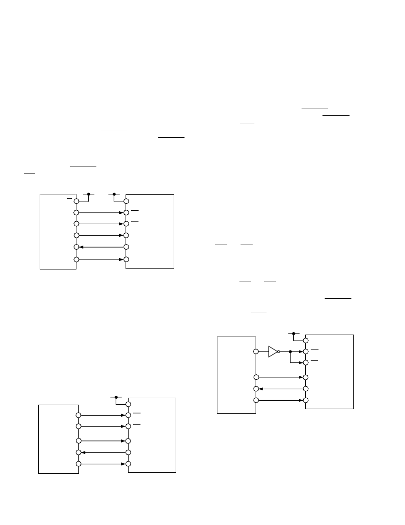
AD7890–DSP56000 Interface
Figure 15 shows an interface circuit between the AD7890 and
the DSP56000 DSP processor. T he AD7890 is configured for
its external clocking mode. T he DSP56000 is configured for
normal mode, synchronous operation with continuous clock. It
is also set up for a 16-bit word with SCK and SC2 as outputs.
T he FSL bit of the DSP56000 should be set to 0.
T he
RFS
and
TFS
inputs of the AD7890 are connected
together so data is transmitted to and from the AD7890 at the
same time. With the DSP56000 in synchronous mode, it pro-
vides a common frame synchronization pulse for read and write
operations on its SC2 output. T his is inverted before being
applied to the
RFS
and
TFS
inputs of the AD7890.
T o monitor the conversion time on the AD7890 a scheme, such
as outlined in previous interface examples with
CONVST
, can
be used. T his can be implemented by connecting the
CONVST
line directly to the
IRQA
input of the DSP56000.
SMODE
TFS
DATA OUT
DATA IN
SCLK
AD7890
RFS
SC2
SCK
DSP56000
DV
DD
SRD
STD
Figure 15. AD7890 to DSP56000 Interface
AD7890–T MS320C25/30 Interface
Figure 16 shows an interface circuit between the AD7890 and
the T MS320C25/30 DSP processor. T he AD7890 is configured
for its Self-Clocking Mode where it provides the serial clock and
frame synchronization signals. However, the T MS320C25/30
requires a continuous serial clock. In the scheme outlined here,
the AD7890’s master clock signal, CLK IN, is used to provide
the serial clock for the processor. T he AD7890’s output SCLK ,
相關PDF資料 |
PDF描述 |
|---|---|
| AD7890AN-2 | Explosion-Proof Limit Switches Series CX: Standard Housing: Side Rotary, Lever not included |
| AD7890AN-4 | Explosion-Proof Limit Switches Series CX: Standard Housing: Side Rotary, Lever not included |
| AD7891YS-1 | LC2MOS 8-Channel, 12-Bit High Speed Data Acquisition System |
| AD7891YS-2 | LC2MOS 8-Channel, 12-Bit High Speed Data Acquisition System |
| AD7891YP-1 | CAT5E PATCH CORD 6 FOOT BEIGE |
相關代理商/技術參數 |
參數描述 |
|---|---|
| AD7891AP1 | 制造商:Analog Devices 功能描述: |
| AD7891AP-1 | 功能描述:IC DAS 12BIT 8CH 44-PLCC RoHS:否 類別:集成電路 (IC) >> 數據采集 - ADCs/DAC - 專用型 系列:- 產品培訓模塊:Lead (SnPb) Finish for COTS Obsolescence Mitigation Program 標準包裝:50 系列:- 類型:數據采集系統(DAS) 分辨率(位):16 b 采樣率(每秒):21.94k 數據接口:MICROWIRE?,QSPI?,串行,SPI? 電壓電源:模擬和數字 電源電壓:1.8 V ~ 3.6 V 工作溫度:-40°C ~ 85°C 安裝類型:表面貼裝 封裝/外殼:40-WFQFN 裸露焊盤 供應商設備封裝:40-TQFN-EP(6x6) 包裝:托盤 |
| AD7891AP-1REEL | 功能描述:IC DAS 12BIT 8CH 44-PLCC RoHS:否 類別:集成電路 (IC) >> 數據采集 - ADCs/DAC - 專用型 系列:- 產品培訓模塊:Lead (SnPb) Finish for COTS Obsolescence Mitigation Program 標準包裝:50 系列:- 類型:數據采集系統(DAS) 分辨率(位):16 b 采樣率(每秒):21.94k 數據接口:MICROWIRE?,QSPI?,串行,SPI? 電壓電源:模擬和數字 電源電壓:1.8 V ~ 3.6 V 工作溫度:-40°C ~ 85°C 安裝類型:表面貼裝 封裝/外殼:40-WFQFN 裸露焊盤 供應商設備封裝:40-TQFN-EP(6x6) 包裝:托盤 |
| AD7891AP2 | 制造商:Analog Devices 功能描述: |
| AD7891AP-2 | 功能描述:IC DAS 12BIT 8CH 44-PLCC RoHS:否 類別:集成電路 (IC) >> 數據采集 - ADCs/DAC - 專用型 系列:- 產品培訓模塊:Lead (SnPb) Finish for COTS Obsolescence Mitigation Program 標準包裝:50 系列:- 類型:數據采集系統(DAS) 分辨率(位):16 b 采樣率(每秒):21.94k 數據接口:MICROWIRE?,QSPI?,串行,SPI? 電壓電源:模擬和數字 電源電壓:1.8 V ~ 3.6 V 工作溫度:-40°C ~ 85°C 安裝類型:表面貼裝 封裝/外殼:40-WFQFN 裸露焊盤 供應商設備封裝:40-TQFN-EP(6x6) 包裝:托盤 |
發布緊急采購,3分鐘左右您將得到回復。