- 您現在的位置:買賣IC網 > PDF目錄373924 > AD7892 (Analog Devices, Inc.) LC2MOS Single Supply, 12-Bit 600 kSPS ADC PDF資料下載
參數資料
| 型號: | AD7892 |
| 廠商: | Analog Devices, Inc. |
| 英文描述: | LC2MOS Single Supply, 12-Bit 600 kSPS ADC |
| 中文描述: | LC2MOS單電源,12位600 ksps模數轉換器 |
| 文件頁數: | 11/14頁 |
| 文件大小: | 144K |
| 代理商: | AD7892 |
AD7892
REV. C
–11–
The designed code transitions occur midway between successive
integer LSB values (i.e., 1/2 LSB, 3/2 LSBs, 5/2 LSBs). Output
coding is two’s complement binary with 1 LSB = FSR/4096 =
20 V/4096 = 4.88 mV for the
±
10 V range and 1 LSB = FSR/
4096 = 10 V/4096 = 2.44 mV for the
±
5 V range. The ideal
input/output transfer function for the AD7892-1 is shown in
Table I.
AD7892-2
The analog input section for the AD7892-2 contains no biasing
resistors. The analog input looks directly into the track/hold
input stage. The analog input range on the V
IN1
input is 0 V to
+2.5 V. The V
IN2
input can be left unconnected but if it is
connected to a potential then that potential must be AGND.
The V
IN1
input connects directly to the input sampling capacitor
of the AD7892-2’s track/hold. The value of this input sampling
capacitor is nominally 10 pF.
Once again, the designed code transitions occur midway be-
tween successive integer LSB values (i.e., 1/2 LSB, 3/2 LSBs,
5/2 LSBs). Output coding is straight (natural) binary with
1 LSB = FSR/4096 = 2.5 V/4096 = 0.61 mV. The ideal input/
output transfer function for the AD7892-2 is shown in Table II.
Table I. Ideal Input/Output Code Table for the AD7892-1
Digital Output
Code Transition
Analog Input
+FSR/2 – 3/2 LSB
1, 2
(9.99268 or 4.99634)
3
+FSR/2 – 5/2 LSBs (9.98779 or 4.99390)
+FSR/2 – 7/2 LSBs (9.98291 or 4.99146)
AGND + 3/2 LSB (0.00732 or 0.00366)
AGND + 1/2 LSB (0.00244 or 0.00122)
AGND – 1/2 LSB (–0.00244 or –0.00122)
AGND – 3/2 LSB (–0.00732 or –0.00366)
–FSR/2 + 5/2 LSB (–9.98779 or –4.99390)
–FSR/2 + 3/2 LSB (–9.99268 or –4.99634)
–FSR/2 + 1/2 LSB (–9.99756 or –4.99878)
011 . . . 110 to 011 . . . 111
011 . . . 101 to 011 . . . 110
011 . . . 100 to 011 . . . 101
000 . . . 001 to 000 . . . 010
000 . . . 000 to 000 . . . 001
111 . . . 111 to 000 . . . 000
111 . . . 110 to 111 . . . 111
100 . . . 010 to 100 . . . 011
100 . . . 001 to 100 . . . 010
100 . . . 000 to 100 . . . 001
NOTES
1
FSR is full-scale range and REF IN = +2.5 V, is 20 V for the
±
10 V range and 10 V
for the
±
5 V range.
2
1 LSB = FSR/4096 = 4.88 mV (
±
10 V range) and 2.44 mV (
±
5 V range) with REF
IN = +2.5 V.
3
±
10 V range or
±
5 V range.
Table II. Ideal Input/Output Code Table for the AD7892-2
Digital Output
Code Transition
Analog Input
+FSR – 3/2 LSB
1, 2
(2.499084 V)
+FSR – 5/2 LSBs (2.498474 V)
+FSR – 7/2 LSBs (2.497864 V)
AGND + 5/2 LSB (0.001526 V)
AGND + 3/2 LSB (0.00916 V)
AGND + 1/2 LSB (0.000305 V)
111 . . . 110 to 111 . . . 111
111 . . . 110 to 111 . . . 110
111 . . . 100 to 111 . . . 101
000 . . . 010 to 010 . . . 011
000 . . . 001 to 001 . . . 010
000 . . . 000 to 000 . . . 001
NOTES
1
FSR is full-scale range and is 2.5 V with REF IN = +2.5 V.
2
1 LSB = FSR/4096 = 0.61 mV with REF IN = +2.5 V.
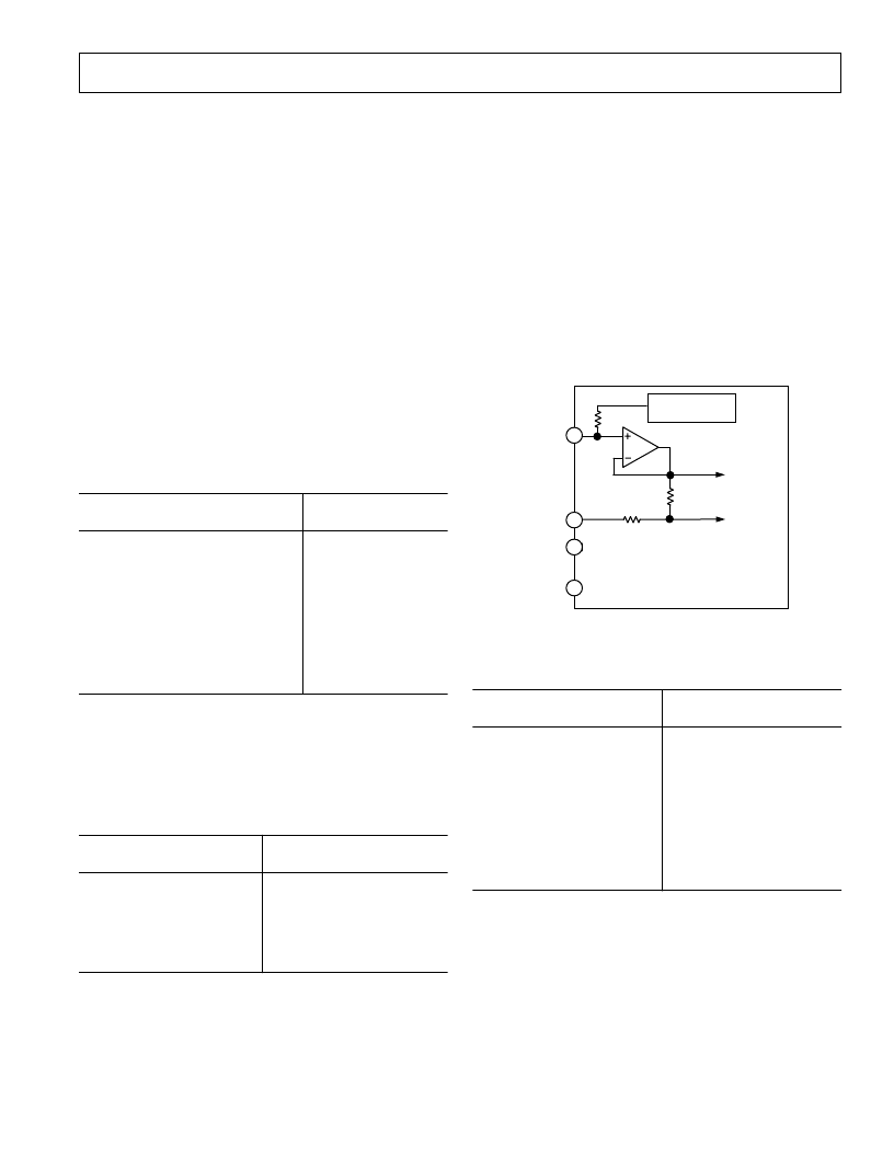
AD7892-3
Figure 5 shows the analog input section for the AD7892-3. The
analog input range is
±
2.5 V on the V
IN1
input. The V
IN2
input
can be left unconnected but if it is connected to a potential then
that potential must be AGND. The input resistance on the V
IN1
is 1.8 k
nominal. As a result, the V
IN1
input should be driven
from a low impedance source. The resistor attenuator stage is
followed by the high input impedance stage of the track/hold
amplifier. This resistor attenuator stage allows the input voltage
to go to
±
7 V without damaging the AD7892-3.
The designed code transitions occur midway between succes-
sive integer LSB values (i.e., 1/2 LSB, 3/2 LSBs, 5/2 LSBs).
Output coding is two’s complement binary with 1 LSB = FSR/
4096 = 5 V/4096 = 1.22 mV with REF IN = +2.5 V. The ideal
input/output transfer function for the AD7892-3 is shown in
Table III.
+2.5
REFERENCE
REF OUT/
REF IN
V
IN1
V
IN2
*
AGND
TO HIGH
IMPEDANCE
SHA INPUT
TO ADC
REFERENCE
CIRCUITRY
2k
3.25k
3.25k
* UNCONNECTED INTERNALLY ON THE AD7892-3
Figure 5. AD7892-3 Analog Input Structure
Table III. Ideal Input/Output Code Table for the AD7892-3
Digital Output
Code Transition
Analog Input
+FSR/2 – 3/2 LSB
1, 2
(2.49817)
+FSR/2 – 5/2 LSBs (2.49695)
+FSR/2 – 7/2 LSBs (2.49573)
AGND + 3/2 LSB (0.00183)
AGND + 1/2 LSB (0.00061)
AGND – 1/2 LSB (–0.00061)
AGND – 3/2 LSB (–0.00183)
–FSR/2 + 5/2 LSB (–2.49695)
–FSR/2 + 3/2 LSB (–2.49817)
–FSR/2 + 1/2 LSB (–2.49939)
011 . . . 110 to 011 . . . 111
011 . . . 110 to 011 . . . 110
011 . . . 110 to 011 . . . 101
000 . . . 001 to 000 . . . 010
000 . . . 000 to 000 . . . 001
111 . . . 111 to 000 . . . 000
111 . . . 110 to 111 . . . 111
100 . . . 010 to 100 . . . 011
100 . . . 001 to 100 . . . 010
100 . . . 000 to 100 . . . 001
NOTES
1
FSR is full-scale range and is 5 V with REF IN = +2.5 V.
2
1 LSB = FSR/4096 = 1.22 mV with REF IN = +2.5 V.
相關PDF資料 |
PDF描述 |
|---|---|
| AD7892AR | RADIATION HARDENED HIGH EFFICIENCY, 5 AMP SWITCHING REGULATORS |
| AD7892AR-3 | LC2MOS Single Supply, 12-Bit 600 kSPS ADC |
| AD7892BR-3 | LC2MOS Single Supply, 12-Bit 600 kSPS ADC |
| AD7892ACHIPS-3 | Ultra-High-Precision SOT23 Series Voltage Reference |
| AD7892BN | LC 2 MOS Single Supply 12-Bit 600 kSPS ADC(144.58 k) |
相關代理商/技術參數 |
參數描述 |
|---|---|
| AD7892A-2REEL | 制造商:Rochester Electronics LLC 功能描述:- Tape and Reel 制造商:Analog Devices 功能描述: |
| AD7892AN-1 | 功能描述:IC ADC 12BIT LP 500KSPS 24-DIP RoHS:否 類別:集成電路 (IC) >> 數據采集 - 模數轉換器 系列:- 標準包裝:1 系列:- 位數:14 采樣率(每秒):83k 數據接口:串行,并聯 轉換器數目:1 功率耗散(最大):95mW 電壓電源:雙 ± 工作溫度:0°C ~ 70°C 安裝類型:通孔 封裝/外殼:28-DIP(0.600",15.24mm) 供應商設備封裝:28-PDIP 包裝:管件 輸入數目和類型:1 個單端,雙極 |
| AD7892AN-2 | 功能描述:IC ADC 12BIT LP 500KSPS 24-DIP RoHS:否 類別:集成電路 (IC) >> 數據采集 - 模數轉換器 系列:- 標準包裝:1 系列:- 位數:14 采樣率(每秒):83k 數據接口:串行,并聯 轉換器數目:1 功率耗散(最大):95mW 電壓電源:雙 ± 工作溫度:0°C ~ 70°C 安裝類型:通孔 封裝/外殼:28-DIP(0.600",15.24mm) 供應商設備封裝:28-PDIP 包裝:管件 輸入數目和類型:1 個單端,雙極 |
| AD7892AN-3 | 制造商:Rochester Electronics LLC 功能描述:12-BIT 600 KSPS ADC I.C. - Bulk 制造商:Analog Devices 功能描述: |
| AD7892ANZ-1 | 功能描述:IC ADC 12BIT LP 500KSPS 24DIP RoHS:是 類別:集成電路 (IC) >> 數據采集 - 模數轉換器 系列:- 標準包裝:1 系列:- 位數:14 采樣率(每秒):83k 數據接口:串行,并聯 轉換器數目:1 功率耗散(最大):95mW 電壓電源:雙 ± 工作溫度:0°C ~ 70°C 安裝類型:通孔 封裝/外殼:28-DIP(0.600",15.24mm) 供應商設備封裝:28-PDIP 包裝:管件 輸入數目和類型:1 個單端,雙極 |
發布緊急采購,3分鐘左右您將得到回復。