- 您現在的位置:買賣IC網 > PDF目錄373924 > AD7892AR (ANALOG DEVICES INC) RADIATION HARDENED HIGH EFFICIENCY, 5 AMP SWITCHING REGULATORS PDF資料下載
參數資料
| 型號: | AD7892AR |
| 廠商: | ANALOG DEVICES INC |
| 元件分類: | ADC |
| 英文描述: | RADIATION HARDENED HIGH EFFICIENCY, 5 AMP SWITCHING REGULATORS |
| 中文描述: | 1-CH 12-BIT SUCCESSIVE APPROXIMATION ADC, SERIAL/PARALLEL ACCESS, PDSO24 |
| 封裝: | SOIC-24 |
| 文件頁數: | 10/14頁 |
| 文件大小: | 144K |
| 代理商: | AD7892AR |
AD7892
–10–
REV. C
pulse can be applied to the
CS
and
RD
inputs to latch data out
of the AD7892 and into the gate array or ASIC. This eliminates
the logic required in the gate array or ASIC to recognize the end
of conversion and generate the read signal for the AD7892. To
obtain optimum performance from the AD7892, it is not recom-
mended to tie
CS
and
RD
permanently low as this keeps the
three-state active during conversion.
Serial Interface Mode
The AD7892 is configured for serial mode interfacing by tying
the MODE input low. It provides for a three-wire, serial link
between the AD7892 and industry-standard microprocessors,
microcontrollers and digital signal processors. SCLK and
RFS
of the AD7892 are inputs, and the AD7892’s serial interface is
designed for direct interface to systems that provide a serial
clock input that is synchronized to the serial data output includ-
ing microcontrollers such as the 80C51, 87C51, 68HC11 and
68HC05 and most digital signal processors.
Figure 3 shows the timing diagram for reading from the AD7892
in the serial interface mode.
RFS
goes low to access data from
the AD7892. The serial clock input does not have to be con-
tinuous. The serial data can be accessed in a number of bytes.
However,
RFS
must remain low for the duration of the data
transfer operation. Sixteen bits of data are transmitted with four
leading zeros followed by the 12-bit conversion result starting
with the MSB. Serial data is clocked out of the device on the
rising edge of SCLK. Old data is guaranteed to be valid for 5 ns
after this edge. This is useful for high speed serial clocks where
the access time of the part would not allow sufficient set-up time
for the data to be accepted on the falling edge of the clock. In
this case, care must be taken that
RFS
does not go just prior to
a rising edge of SCLK. For slower serial clocks data is valid on
the falling edge of SCLK. At the end of the read operation, the
SDATA line is three-stated by a rising edge on either the SCLK
or
RFS
inputs, whichever occurs first. Serial data cannot be
read during conversion to avoid feedthrough problems from the
serial clock to the conversion process. For optimum perfor-
mance of the AD7892-3, a serial read should also be avoided
within 200 ns of the rising edge of
CONVST
to avoid feedthrough
into the track/hold during its acquisition time. The serial read
should, therefore, occur between the end of conversion (
EOC
falling edge) and 200 ns prior to the next rising edge of
CONVST
. For the AD7892-1 and AD7892-2, a serial read
should also be avoided within 400 ns of the rising edge of
CONVST
. This limits the maximum achievable throughput
rate in serial mode (assuming 20 MHz serial clock) to 400 kSPS
for the AD7892-3 and 357 kSPS for the AD7892-1 and
AD7892-2.
Analog Input Section
The AD7892 is offered as three part types allowing for four
different analog input voltage ranges. The AD7892-1 handles
either
±
5 V or
±
10 V input voltage ranges. The AD7892-2
handles a 0 V to +2.5 V input voltage range while the AD7892-3
handles an input range of
±
2.5 V.
AD7892-1
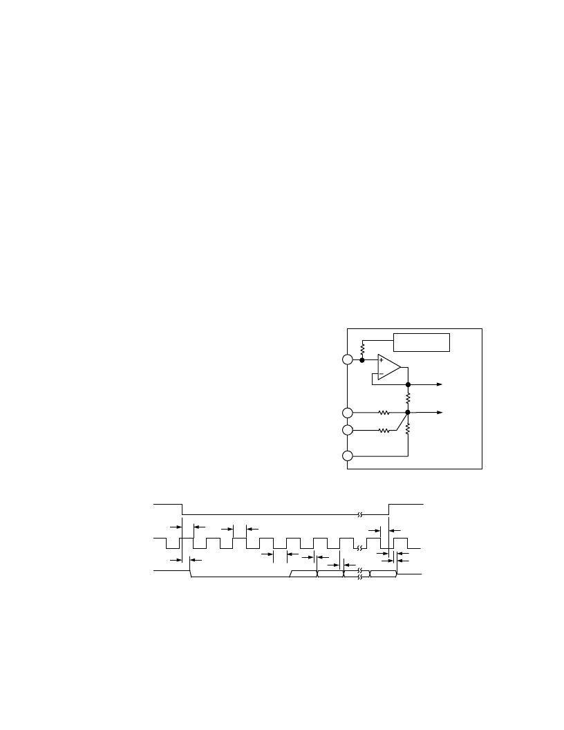
Figure 4 shows the analog input section for the AD7892-1. The
analog input range is pin-strappable (using V
IN2
) for either
±
5 V
or
±
10 V on the V
IN1
input. With V
IN2
connected to AGND, the
input range on V
IN1
is
±
10 V, and the input resistance on V
IN1
is
15 k
nominal. With V
IN2
connected to V
IN1
, the input range on
V
IN1
is
±
5 V, and the input resistance on V
IN1
is 8 k
nominal.
As a result, the V
IN1
and V
IN2
inputs should be driven from a
low impedance source. The resistor attenuator stage is followed
by the high input impedance stage of the track/hold amplifier.
This resistor attenuator stage allows the input voltage to go to
±
17 V without damaging the AD7892-1.
+2.5
REFERENCE
REF OUT/
REF IN
V
IN1
V
IN2
AGND
TO HIGH
IMPEDANCE
SHA INPUT
TO ADC
REFERENCE
CIRCUITRY
2k
3.25k
13k
6.5k
13k
Figure 4. AD7892-1 Analog Input Structure
t
13
t
10
THREE-
STATE
RFS
(I)
SCLK (I)
SDATA (O)
NOTE:
I = INPUT; O = OUTPUT
FOUR LEADING ZEROS
t
12
t
11
t
16
t
17
t
17A
t
14
DB11
DB10
DB0
t
15
Figure 3. Serial Mode Timing Diagram
相關PDF資料 |
PDF描述 |
|---|---|
| AD7892AR-3 | LC2MOS Single Supply, 12-Bit 600 kSPS ADC |
| AD7892BR-3 | LC2MOS Single Supply, 12-Bit 600 kSPS ADC |
| AD7892ACHIPS-3 | Ultra-High-Precision SOT23 Series Voltage Reference |
| AD7892BN | LC 2 MOS Single Supply 12-Bit 600 kSPS ADC(144.58 k) |
| AD7892BR | Dual High Efficiency, Low Noise, Synchronous Step-Down Switching Regulators |
相關代理商/技術參數 |
參數描述 |
|---|---|
| AD7892AR-1 | 功能描述:IC ADC 12BIT LP 500KSPS 24-SOIC RoHS:否 類別:集成電路 (IC) >> 數據采集 - 模數轉換器 系列:- 標準包裝:1 系列:- 位數:14 采樣率(每秒):83k 數據接口:串行,并聯 轉換器數目:1 功率耗散(最大):95mW 電壓電源:雙 ± 工作溫度:0°C ~ 70°C 安裝類型:通孔 封裝/外殼:28-DIP(0.600",15.24mm) 供應商設備封裝:28-PDIP 包裝:管件 輸入數目和類型:1 個單端,雙極 |
| AD7892AR-1REEL | 功能描述:IC ADC 12BIT LP 500KSPS 24-SOIC RoHS:否 類別:集成電路 (IC) >> 數據采集 - 模數轉換器 系列:- 標準包裝:1,000 系列:- 位數:12 采樣率(每秒):300k 數據接口:并聯 轉換器數目:1 功率耗散(最大):75mW 電壓電源:單電源 工作溫度:0°C ~ 70°C 安裝類型:表面貼裝 封裝/外殼:24-SOIC(0.295",7.50mm 寬) 供應商設備封裝:24-SOIC 包裝:帶卷 (TR) 輸入數目和類型:1 個單端,單極;1 個單端,雙極 |
| AD7892AR-1Z | 制造商:Analog Devices 功能描述:IC, 12BIT ADC 600KSPS, SMD, WSOIC24 |
| AD7892AR-2 | 功能描述:IC ADC 12BIT LP 500KSPS 24-SOIC RoHS:否 類別:集成電路 (IC) >> 數據采集 - 模數轉換器 系列:- 標準包裝:1 系列:- 位數:14 采樣率(每秒):83k 數據接口:串行,并聯 轉換器數目:1 功率耗散(最大):95mW 電壓電源:雙 ± 工作溫度:0°C ~ 70°C 安裝類型:通孔 封裝/外殼:28-DIP(0.600",15.24mm) 供應商設備封裝:28-PDIP 包裝:管件 輸入數目和類型:1 個單端,雙極 |
| AD7892AR-2REEL | 制造商:Analog Devices 功能描述:ADC Single SAR 500ksps 12-bit Parallel/Serial 24-Pin SOIC W T/R 制造商:Rochester Electronics LLC 功能描述:12-BIT 500 KSPS PARALLEL ADC I.C. - Tape and Reel |
發布緊急采購,3分鐘左右您將得到回復。