- 您現在的位置:買賣IC網 > PDF目錄373925 > AD7894 (Analog Devices, Inc.) 5 V, 14-Bit Serial, 5 ms ADC in SO-8 Package PDF資料下載
參數資料
| 型號: | AD7894 |
| 廠商: | Analog Devices, Inc. |
| 英文描述: | 5 V, 14-Bit Serial, 5 ms ADC in SO-8 Package |
| 中文描述: | 5伏,14位序列,5毫秒ADC的SO - 8封裝 |
| 文件頁數: | 7/12頁 |
| 文件大小: | 131K |
| 代理商: | AD7894 |
AD7894
–7–
REV. 0
Track/Hold Section
The track/hold amplifier on the analog input of the AD7894
allows the ADC to accurately convert an input sine wave of full-
scale amplitude to 14-bit accuracy. The input bandwidth of the
track/hold is greater than the Nyquist rate of the ADC, even
when the ADC is operated at its maximum throughput rate of
160 kHz (i.e., the track/hold can handle input frequencies in
excess of 100 kHz).
The track/hold amplifier acquires an input signal to 14-bit accu-
racy in less than 0.35
μ
s. The operation of the track/hold is
essentially transparent to the user. With the high sampling
operating mode the track/hold amplifier goes from its tracking
mode to its hold mode at the start of conversion (i.e., the falling
edge of
CONVST
). The aperture time for the track/hold (i.e.,
the delay time between the external
CONVST
signal and the
track/hold actually going into hold) is typically 15ns. At the
end of conversion (on the falling edge of BUSY) the part re-
turns to its tracking mode. The acquisition time of the track/
hold amplifier begins at this point. For the auto shutdown mode,
the rising edge of
CONVST
wakes up the part and the track
and hold amplifier goes from its tracking mode to its hold mode
5
μ
s after the rising edge of
CONVST
(provided that the
CONVST
high time is less than 5
μ
s). Once again the part re-
turns to its tracking mode at the end of conversion when the
BUSY signal goes low.
Reference Input
The reference input to the AD7894 is buffered on-chip with a
maximum reference input current of 1
μ
A. The part is specified
with a +2.5 V reference input voltage. Errors in the reference
source will result in gain errors in the AD7894’s transfer func-
tion and will add to the specified full-scale errors on the part.
Suitable reference sources for the AD7894 include the AD780
and AD680 precision +2.5 V references.
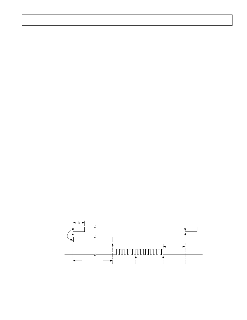
Timing and Control Section
Figure 3 shows the timing and control sequence required to
obtain optimum performance from the AD7894. In the se-
quence shown, conversion is initiated on the falling edge of
CONVST
and new data from this conversion is available in the
output register of the AD7894 5
μ
s later. Once the read opera-
tion has taken place, a further 250ns should be allowed before
the next falling edge of
CONVST
to optimize the settling of the
track/hold amplifier before the next conversion is initiated.
With the serial clock frequency at its maximum of 16MHz, the
achievable throughput rate for the part is 5
μ
s (conversion
time) plus 1.0
μ
s (read time) plus 250ns (quiet time). This
results in a minimum throughput time of 6.25
μ
s (equivalent to
a throughput rate of 160 kHz). A serial clock of less than 16MHz
can be used, but this will in turn mean that the throughput
time will increase.
The read operation consists of 16 serial clock pulses to the
output shift register of the AD7894. After 16 serial clock pulses
the shift register is reset and the SDATA line is three-stated. If
there are more serial clock pulses after the 16th clock, the shift
register will be moved on past its reset state. However, the shift
register will be reset again on the falling edge of the
CONVST
signal to ensure that the part returns to a known state every
conversion cycle. As a result, a read operation from the output
register should not straddle across the falling edge of
CONVST
as the output shift register will be reset in the middle of the
read operation and the data read back into the microprocessor
will appear invalid.
OPERATING MODES
Mode 1 Operation (High Sampling Performance)
The timing diagram in Figure 3 is for optimum performance in
operating Mode 1 where the falling edge of
CONVST
starts
conversion and puts the Track/Hold amplifier into its hold
mode. This falling edge of
CONVST
also causes the BUSY
signal to go high to indicate that a conversion is taking place.
The BUSY signal goes low when the conversion is complete,
which is 5
μ
s max after the falling edge of
CONVST
and new
data from this conversion is available in the output register of
the AD7894. A read operation accesses this data. This read
operation consists of 16 clock cycles and the length of this read
operation will depend on the serial clock frequency. For the
fastest throughput rate (with a serial clock of 16 MHz) the read
operation will take 1.0
μ
s. The read operation must be com-
plete at least 250 ns before the falling edge of the next
CONVST
and this gives a total time of 6.25
μ
s for the full throughput
time (equivalent to 160 kHz). This mode of operation should
be used for high sampling applications.
250ns MIN
t
1
= 40ns MIN
t
CONVERT
= 5
m
s
BUSY
SCLK
CONVST
CONVERSION IS
INITIATED;
TRACK/HOLD
GOES INTO HOLD
CONVERSION
ENDS
5
m
s LATER
SERIAL READ
OPERATION
READ OPERATION
SHOULD END
250ns PRIOR TO
NEXT FALLING
EDGE OF
CONVST
OUTPUT
SERIAL
SHIFT
REGISTER
IS RESET
Figure 3. Mode 1 Timing Operation Diagram for High Sampling Performance
相關PDF資料 |
PDF描述 |
|---|---|
| AD7894AR-10 | Metal Oxide Varistor (MOV); Voltage Rating AC, Vrms:130Vrms; Voltage Rating DC, Vdc:170VDC; Peak Surge Current (8/20uS), Itm:6000A; Clamping Voltage 8/20us Max :340V; Capacitance, Cd:650pF; Package/Case:14mm Disc |
| AD7894AR-2 | VARISTOR 30VRMS 14MM RADIAL |
| AD7894AR-3 | VARISTOR 320V RMS 14MM RADIAL |
| AD7894BR-10 | SWITCH SLIDE SPDT R/A .5A PCB |
| AD7894BR-3 | SWITCH SLIDE SPDT .3A SMD |
相關代理商/技術參數 |
參數描述 |
|---|---|
| AD7894AR-10 | 功能描述:IC ADC 14BIT SRL T/H LP 8-SOIC RoHS:否 類別:集成電路 (IC) >> 數據采集 - 模數轉換器 系列:- 標準包裝:1,000 系列:- 位數:12 采樣率(每秒):300k 數據接口:并聯 轉換器數目:1 功率耗散(最大):75mW 電壓電源:單電源 工作溫度:0°C ~ 70°C 安裝類型:表面貼裝 封裝/外殼:24-SOIC(0.295",7.50mm 寬) 供應商設備封裝:24-SOIC 包裝:帶卷 (TR) 輸入數目和類型:1 個單端,單極;1 個單端,雙極 |
| AD7894AR-10REEL | 制造商:Analog Devices 功能描述:ADC Single SAR 200ksps 14-bit Serial 8-Pin SOIC N T/R 制造商:Analog Devices 功能描述:ADC SGL SAR 200KSPS 14BIT SERL 8SOIC N - Tape and Reel |
| AD7894AR-10REEL7 | 功能描述:IC ADC 14BIT SRL T/H LP 8-SOIC RoHS:否 類別:集成電路 (IC) >> 數據采集 - 模數轉換器 系列:- 標準包裝:1,000 系列:- 位數:12 采樣率(每秒):300k 數據接口:并聯 轉換器數目:1 功率耗散(最大):75mW 電壓電源:單電源 工作溫度:0°C ~ 70°C 安裝類型:表面貼裝 封裝/外殼:24-SOIC(0.295",7.50mm 寬) 供應商設備封裝:24-SOIC 包裝:帶卷 (TR) 輸入數目和類型:1 個單端,單極;1 個單端,雙極 |
| AD7894AR-10Z | 制造商:Analog Devices 功能描述:ADC 14BIT 5V 7.5MHZ 2LSB 制造商:Analog Devices 功能描述:ADC, 14BIT, 5V, 7.5MHZ, 2LSB, 8SOIC; Resolution (Bits):14bit; Sampling Rate:200kSPS; Supply Voltage Type:Single; Supply Voltage Min:4.75V; Supply Voltage Max:5.25V; Supply Current:5.5mA; Digital IC Case Style:NSOIC; No. of Pins:8; ;RoHS Compliant: Yes |
| AD7894AR-2 | 制造商:Analog Devices 功能描述:ADC Single SAR 200ksps 14-bit Serial 8-Pin SOIC N 制造商:Analog Devices 功能描述:CONVERTOR AD ((NW)) |
發布緊急采購,3分鐘左右您將得到回復。