- 您現在的位置:買賣IC網 > PDF目錄373925 > AD7894BR-10 (ANALOG DEVICES INC) SWITCH SLIDE SPDT R/A .5A PCB PDF資料下載
參數資料
| 型號: | AD7894BR-10 |
| 廠商: | ANALOG DEVICES INC |
| 元件分類: | ADC |
| 英文描述: | SWITCH SLIDE SPDT R/A .5A PCB |
| 中文描述: | 1-CH 14-BIT SUCCESSIVE APPROXIMATION ADC, SERIAL ACCESS, PDSO8 |
| 封裝: | SOIC-8 |
| 文件頁數: | 8/12頁 |
| 文件大小: | 131K |
| 代理商: | AD7894BR-10 |
AD7894
–8–
REV. 0
250ns MIN
BUSY
SCLK
CONVST
CONVERSION
IS INITIATED;
TRACK/HOLD
GOES INTO
HOLD
CONVERSION
ENDS
10
m
s LATER
SERIAL READ
OPERATION
READ OPERATION
SHOULD END 250ns
PRIOR TO NEXT
RISING EDGE OF
CONVST
OUTPUT
SERIAL SHIFT
REGISTER
IS RESET
t
CONVERT
= 10
m
s
PART
WAKES
UP
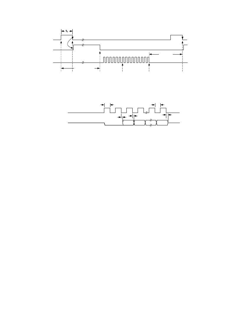
Figure 4. Mode 2 Timing Diagram Where Automatic Sleep Function is Initiated
t
2
t
3
t
4
t
5
t
6
2 LEADING
ZEROS
THREE-STATE
THREE-
STATE
1
2
3
4
15
16
DB13
DB12
DB0
SCLK (I/P)
DOUT (O/P)
t
2
=
t
3
= 31.25ns MIN,
t
4
= 60ns MAX,
t
5
= 10ns MIN,
t
6
= 20ns MAX @ 5V, A, B, VERSIONS
Figure 5. Data Read Operation
Mode 2 Operation (Auto Sleep After Conversion)
The timing diagram in Figure 4 is for optimum performance in
operating Mode 2, where the part automatically goes into sleep
mode once BUSY goes low, after conversion and “wakes up”
before the next conversion takes place. This is achieved by keep-
ing
CONVST
low at the end of conversion, whereas it was high
at the end of conversion for Mode 1 Operation. The rising edge
of
CONVST
“wakes up” the AD7894. This wake-up time is
typically 5
μ
s and is controlled internally by a monostable cir-
cuit. While the AD7894 is waking up there is some digital activ-
ity internal to the part. If the falling edge of
CONVST
(putting
the track/hold amplifier into hold mode) should occur during
this digital activity, noise will be injected into the track/hold
amplifier resulting in a poor conversion. For optimum results
the
CONVST
pulse should be between 40 ns and 2
μ
s or greater
than 6
μ
s in width. The narrower pulse will allow a system to
instruct the AD7894 to begin waking up and perform a conver-
sion when ready, whereas the pulse greater than 6
μ
s will give
control over when the sampling instant takes place. Note that
the 10
μ
s wake-up time shown in Figure 4 is for a
CONVST
pulse
less than 2
μ
s. If a
CONVST
pulse greater than 6
μ
s is used, the
conversion will not complete for a further 5
μ
s after the falling edge
of
CONVST
. Even though the part is in sleep mode, data can still
be read from it. The read operation consists of 16 clock cycles as in
Mode 1 Operation. For the fastest serial clock of 16 MHz, the read
operation will take 1.0
μ
s and this must be complete at least 250 ns
before the falling edge of the next
CONVST
, to allow the track/
hold amplifier to have enough time to settle. This mode is very
useful when the part is converting at a slow rate, as the power
consumption will be significantly reduced from that of Mode 1
Operation.
Serial Interface
The serial interface to the AD7894 consists of just three wires, a
serial clock input (SCLK) and the serial data output (SDATA)
and a conversion status output (BUSY). This allows for an
easy-to-use interface to most microcontrollers, DSP processors
and shift registers.
Figure 5 shows the timing diagram for the read operation to the
AD7894. The serial clock input (SCLK) provides the clock
source for the serial interface. Serial data is clocked out from
the SDATA line on the falling edge of this clock and is valid on
both the rising and falling edges of SCLK. The advantage of
having the data valid on both the rising and falling edges of the
SCLK is to give the user greater flexibility in interfacing to the
part and so a wider range of microprocessor and microcontrol-
ler interfaces can be accommodated. This also explains the two
timing figures, t
4
and t
5
, that are quoted on the diagram. The
time t
4
specifies how long after the falling edge of the SCLK the
next data bit becomes valid, whereas the time t
5
specifies for
how long after the falling edge of the SCLK the current data bit
is valid. The first leading zero is clocked out on the first rising
edge of SCLK. Note that the first zero will be valid on the first
falling edge of SCLK even though the data access time is speci-
fied at 60 ns for the other bits. The reason for this is that the
first bit will be clocked out faster than the other bits is due to
the internal architecture of the part. Sixteen clock pulses must
be provided to the part to access to full conversion result. The
AD7894 provides two leading zeros followed by the 14-bit
conversion result starting with the MSB (DB13). The last data
bit to be clocked out on the penultimate falling clock edge is the
LSB (DB0). On the 16th falling edge of SCLK the LSB (DB0)
will be valid for a specified time to allow the bit to be read on
the falling edge of the SCLK and then the SDATA line is dis-
abled (three-stated). After this last bit has been clocked out,
the SCLK input should return low and remain low until the
next serial data read operation. If there are extra clock pulses
after the 16th clock, the AD7894 will start over again with
outputting data from its output register and the data bus will
no longer be three-stated even when the clock stops. Provided
the serial clock has stopped before the next falling edge of
相關PDF資料 |
PDF描述 |
|---|---|
| AD7894BR-3 | SWITCH SLIDE SPDT .3A SMD |
| AD7895AN-3 | 5 V, 12-Bit, Serial 3.8 ms ADC in 8-Pin Package |
| AD7895AR-10 | 5 V, 12-Bit, Serial 3.8 ms ADC in 8-Pin Package |
| AD7895AR-2 | 5 V, 12-Bit, Serial 3.8 ms ADC in 8-Pin Package |
| AD7895AR-3 | 5 V, 12-Bit, Serial 3.8 ms ADC in 8-Pin Package |
相關代理商/技術參數 |
參數描述 |
|---|---|
| AD7894BR-10REEL | 制造商:Analog Devices 功能描述:ADC Single SAR 200ksps 14-bit Serial 8-Pin SOIC N T/R |
| AD7894BR-10REEL7 | 制造商:Analog Devices 功能描述:ADC Single SAR 200ksps 14-bit Serial 8-Pin SOIC N T/R |
| AD7894BR-3 | 功能描述:IC ADC 14BIT SRL T/H LP 8-SOIC RoHS:否 類別:集成電路 (IC) >> 數據采集 - 模數轉換器 系列:- 產品培訓模塊:Lead (SnPb) Finish for COTS Obsolescence Mitigation Program 標準包裝:2,500 系列:- 位數:12 采樣率(每秒):3M 數據接口:- 轉換器數目:- 功率耗散(最大):- 電壓電源:- 工作溫度:- 安裝類型:表面貼裝 封裝/外殼:SOT-23-6 供應商設備封裝:SOT-23-6 包裝:帶卷 (TR) 輸入數目和類型:- |
| AD7894BR-3REEL | 功能描述:IC ADC 14BIT SRL T/H LP 8-SOIC RoHS:否 類別:集成電路 (IC) >> 數據采集 - 模數轉換器 系列:- 標準包裝:1,000 系列:- 位數:12 采樣率(每秒):300k 數據接口:并聯 轉換器數目:1 功率耗散(最大):75mW 電壓電源:單電源 工作溫度:0°C ~ 70°C 安裝類型:表面貼裝 封裝/外殼:24-SOIC(0.295",7.50mm 寬) 供應商設備封裝:24-SOIC 包裝:帶卷 (TR) 輸入數目和類型:1 個單端,單極;1 個單端,雙極 |
| AD7894BR-3REEL7 | 制造商:Analog Devices 功能描述:ADC Single SAR 200ksps 14-bit Serial 8-Pin SOIC N T/R |
發布緊急采購,3分鐘左右您將得到回復。