- 您現(xiàn)在的位置:買賣IC網(wǎng) > PDF目錄373925 > AD7895AN-2 (ANALOG DEVICES INC) 5 V, 12-Bit, Serial 3.8 ms ADC in 8-Pin Package PDF資料下載
參數(shù)資料
| 型號: | AD7895AN-2 |
| 廠商: | ANALOG DEVICES INC |
| 元件分類: | ADC |
| 英文描述: | 5 V, 12-Bit, Serial 3.8 ms ADC in 8-Pin Package |
| 中文描述: | 1-CH 12-BIT SUCCESSIVE APPROXIMATION ADC, SERIAL ACCESS, PDIP8 |
| 封裝: | 0.300 INCH, MINI, PLASTIC, DIP-8 |
| 文件頁數(shù): | 10/12頁 |
| 文件大小: | 314K |
| 代理商: | AD7895AN-2 |
AD7895
–10–
REV. 0
AD7895
SDATA
SCLK
BUSY
SCLK1
DR1
ADSP-2103/5
IRQ2
RFS1
Figure 8. AD7896 to ADSP-2103 /5 Interface
The timing relationship between the SCLK1 and RFS1 outputs
of the ADSP-2103/5 are such that the delay between the rising
edge of the SCLK1 and the rising edge of an active high RFS1
is up to 30 ns. There is also a requirement that data must be
set up 10 ns prior to the falling edge of the SCLK1 to be read
correctly by the ADSP-2103/5. The data access time for the
AD7895 is 60 ns (5 V (A, B versions)) from the rising edge of
its SCLK input. Assuming a 10 ns propagation delay through
the external AND gate, the high time of the SCLK1 output of
the ADSP-2105 must be
≥
(30 + 60 +10 +10) ns, i.e.,
≥
110 ns.
This means that the serial clock frequency with which the
interface of Figure 8 can work is limited to 4.5 MHz. However,
there is an alternative method that allows for the ADSP-2105
SCLK1 to run at 5 MHz (the max serial clock frequency of the
SCLK1 output). The arrangement occurs when the first leading
zero of the data stream from the AD7895 cannot be guaranteed
to be clocked into the ADSP-2105 due to the combined delay of
the RFS signal and the data access time of the AD7895. In most
cases, this is acceptable because there will still be three leading
zeros followed by the 12 data bits. For the ADSP-2103, the
SCLK1 frequency will need to be limited to < 4 MHz to
account for the 100 ns data access time of the AD7895.
Another alternative scheme is to configure the ADSP-2103/5 so
that it accepts an external noncontinuous serial clock. In this
case, an external noncontinuous serial clock is provided that
drives the serial clock inputs of both the ADSP-2103/5 and the
AD7895. In this scheme, the serial clock frequency is limited to
15 MHz by the AD7895.
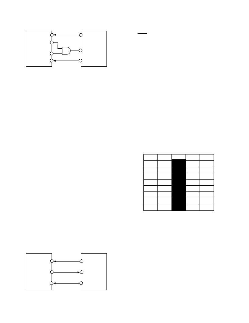
AD7895–DSP56002/L002 Interface
Figure 9 shows an interface circuit between the AD7895 and the
DSP56002/L002 DSP processor. The DSP56002/L002 is
configured for normal mode asynchronous operation with gated
clock. It is also set up for a 16-bit word with SCK as gated
clock output. In this mode, the DSP56002/L002 provides
sixteen serial clock pulses to the AD7895 in a serial read
operation. Because the DSP56002/L002 assumes valid data on
the first falling edge of SCK, the interface is simply two-wire as
shown in Figure 9.
AD7895
SDATA
SCLK
BUSY
SCK
SDR
DSP56002/L002
MODA /
IRQA
Figure 9. AD7895 to DSP56002/L002 Interface
Because the BUSY line from the AD7895 is connected to the
MODA/
IRQA
input of the DSP56002/L002, an interrupt will
be generated at the end of conversion. This ensures that the
read operation will take place after conversion is finished.
AD7895 PERFORMANCE
Linearity
The linearity of the AD7895 is determined by the on-chip
12-bit D/A converter. This is a segmented DAC that is laser
trimmed for 12-bit integral linearity and differential linearity.
Typical relative accuracy numbers for the part are
±
1/4 LSB
while the typical DNL errors are
±
1/2 LSB.
Noise
In an A/D converter, noise exhibits itself as code uncertainty in
dc applications and as the noise floor (in an FFT, for example)
in ac applications. In a sampling A/D converter like the AD7895,
all information about the analog input appears in the baseband
from dc to 1/2 the sampling frequency. The input bandwidth of
the track/hold exceeds the Nyquist bandwidth and, therefore, an
antialiasing filter should be used to remove unwanted signals above
f
S
/2 in the input signal in applications where such signals exist.
Figure 10 shows a histogram plot for 8192 conversions of a dc
input using the AD7895. The analog input was set at the center
of a code transition. It can be seen that almost all the codes
appear in the one output bin, indicating very good noise
performance from the ADC.
957
962
958
959
960
961
0
4000
3000
2000
1000
6000
5000
7000
8000
9000
Figure 10. Histogram of 8192 Conversions of a DC Input
In this case where the output data read for the device occurs
during conversion, this has the effect of injecting noise onto the
die while bit decisions are being made, and this increases the
noise generated by the AD7895. A histogram plot for 8192
conversions of the same dc input would show a larger spread of
codes with the rms noise for the AD7895 increasing. This effect
will vary depending on where the serial clock edges appear with
respect to the bit trials of the conversion process. It is possible
to achieve the same level of performance when reading during
conversion as when reading after conversion, depending on the
relationship of the serial clock edges to the bit trial points.
相關(guān)PDF資料 |
PDF描述 |
|---|---|
| AD7895BR-10 | 5 V, 12-Bit, Serial 3.8 ms ADC in 8-Pin Package |
| AD7895BR-2 | 5 V, 12-Bit, Serial 3.8 ms ADC in 8-Pin Package |
| AD7896JR | 2.7 V to 5.5 V, 12-Bit, 8 us ADC in 8-Pin SO/DIP |
| AD7896 | 2.7 V to 5.5 V, 12-Bit, 8 us ADC in 8-Pin SO/DIP |
| AD7896AN | 14-Bit 50 kSPS ADC Ser. Out, 1.8V Operation 8-MSOP |
相關(guān)代理商/技術(shù)參數(shù) |
參數(shù)描述 |
|---|---|
| AD7895AN-3 | 制造商:Analog Devices 功能描述:ADC Single SAR 192ksps 12-bit Serial 8-Pin PDIP 制造商:Rochester Electronics LLC 功能描述:SERIAL 12 BIT BIPOLAR ADC I.C. - Bulk 制造商:Analog Devices 功能描述:IC 12-BIT ADC |
| AD7895ANZ-10 | 功能描述:IC ADC 12BIT SRL 5V 8DIP RoHS:是 類別:集成電路 (IC) >> 數(shù)據(jù)采集 - 模數(shù)轉(zhuǎn)換器 系列:- 其它有關(guān)文件:TSA1204 View All Specifications 標(biāo)準(zhǔn)包裝:1 系列:- 位數(shù):12 采樣率(每秒):20M 數(shù)據(jù)接口:并聯(lián) 轉(zhuǎn)換器數(shù)目:2 功率耗散(最大):155mW 電壓電源:模擬和數(shù)字 工作溫度:-40°C ~ 85°C 安裝類型:表面貼裝 封裝/外殼:48-TQFP 供應(yīng)商設(shè)備封裝:48-TQFP(7x7) 包裝:Digi-Reel® 輸入數(shù)目和類型:4 個(gè)單端,單極;2 個(gè)差分,單極 產(chǎn)品目錄頁面:1156 (CN2011-ZH PDF) 其它名稱:497-5435-6 |
| AD7895ANZ-2 | 功能描述:IC ADC 12BIT SRL 5V 8DIP RoHS:是 類別:集成電路 (IC) >> 數(shù)據(jù)采集 - 模數(shù)轉(zhuǎn)換器 系列:- 其它有關(guān)文件:TSA1204 View All Specifications 標(biāo)準(zhǔn)包裝:1 系列:- 位數(shù):12 采樣率(每秒):20M 數(shù)據(jù)接口:并聯(lián) 轉(zhuǎn)換器數(shù)目:2 功率耗散(最大):155mW 電壓電源:模擬和數(shù)字 工作溫度:-40°C ~ 85°C 安裝類型:表面貼裝 封裝/外殼:48-TQFP 供應(yīng)商設(shè)備封裝:48-TQFP(7x7) 包裝:Digi-Reel® 輸入數(shù)目和類型:4 個(gè)單端,單極;2 個(gè)差分,單極 產(chǎn)品目錄頁面:1156 (CN2011-ZH PDF) 其它名稱:497-5435-6 |
| AD7895ANZ-3 | 功能描述:IC ADC 12BIT SRL 5V 8DIP RoHS:是 類別:集成電路 (IC) >> 數(shù)據(jù)采集 - 模數(shù)轉(zhuǎn)換器 系列:- 標(biāo)準(zhǔn)包裝:1,000 系列:- 位數(shù):12 采樣率(每秒):300k 數(shù)據(jù)接口:并聯(lián) 轉(zhuǎn)換器數(shù)目:1 功率耗散(最大):75mW 電壓電源:單電源 工作溫度:0°C ~ 70°C 安裝類型:表面貼裝 封裝/外殼:24-SOIC(0.295",7.50mm 寬) 供應(yīng)商設(shè)備封裝:24-SOIC 包裝:帶卷 (TR) 輸入數(shù)目和類型:1 個(gè)單端,單極;1 個(gè)單端,雙極 |
| AD7895AR-10 | 制造商:Analog Devices 功能描述:ADC Single SAR 192ksps 12-bit Serial 8-Pin SOIC N 制造商:Analog Devices 功能描述:ADC SGL SAR 192KSPS 12-BIT SERL 8SOIC N - Rail/Tube 制造商:Analog Devices 功能描述:IC 12-BIT ADC |
發(fā)布緊急采購,3分鐘左右您將得到回復(fù)。