- 您現在的位置:買賣IC網 > PDF目錄373925 > AD7895AR-10 (ANALOG DEVICES INC) 5 V, 12-Bit, Serial 3.8 ms ADC in 8-Pin Package PDF資料下載
參數資料
| 型號: | AD7895AR-10 |
| 廠商: | ANALOG DEVICES INC |
| 元件分類: | ADC |
| 英文描述: | 5 V, 12-Bit, Serial 3.8 ms ADC in 8-Pin Package |
| 中文描述: | 1-CH 12-BIT SUCCESSIVE APPROXIMATION ADC, SERIAL ACCESS, PDSO8 |
| 封裝: | SOIC-8 |
| 文件頁數: | 4/12頁 |
| 文件大小: | 314K |
| 代理商: | AD7895AR-10 |
AD7895
–4–
REV. 0
PIN FUNCTION DESCRIPTION
Pin
No.
Pin
Mnemonic
Description
1
REF IN
Voltage Reference Input. An external reference source should be connected to this pin to provide the refer-
ence voltage for the AD7895’s conversion process. The REF IN input is buffered on chip. The nominal ref-
erence voltage for correct operation of the AD7895 is +2.5 V.
Analog Input Channel. The analog input range is
±
10 V (AD7895-10),
±
2.5 V (AD7895-3) and 0 V to
+2.5 V (AD7895-2).
Analog Ground. Ground reference for track/hold, comparator, digital circuitry and DAC.
Serial Clock Input. An external serial clock is applied to this input to obtain serial data from the AD7895.
A new serial data bit is clocked out on the falling edge of this serial clock. Data is guaranteed valid for 10 ns
after this falling edge so that data can be accepted on the falling edge when a fast serial clock is used. The
serial clock input should be taken low at the end of the serial data transmission.
Serial Data Output. Serial data from the AD7895 is provided at this output. The serial data is clocked out
by the falling edge of SCLK, but the data can also be read on the falling edge of SCLK. This is possible
because data bit N is valid for a specified time after the falling edge of SCLK (data hold time) (see Figure 4).
Sixteen bits of serial data are provided with four leading zeros followed by the 12 bits of conversion data.
On the sixteenth falling edge of SCLK, the SDATA line is held for the data hold time and then is disabled
(three-stated). Output data coding is 2s complement for the AD7895-10, AD7895-3 and straight binary for
the AD7895-2.
The BUSY pin is used to indicate when the part is doing a conversion. The BUSY pin will go high on the
falling edge of
CONVST
and will return low when the conversion is complete.
Convert Start. Edge-triggered logic input. On the falling edge of this input, the track/hold goes into its hold
mode, and conversion is initiated. If
CONVST
is low at the end of conversion, the part goes into power-
down mode. In this case, the rising edge of
CONVST
“wakes up” the part.
Positive supply voltage, +5 V
±
5%.
2
V
IN
3
4
GND
SCLK
5
SDATA
6
BUSY
7
CONVST
8
V
DD
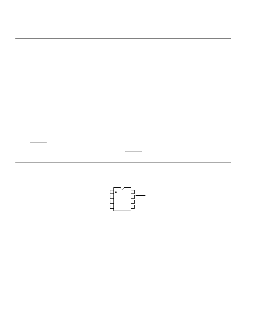
PIN CONFIGURATION
DIP and SOIC
1
2
3
4
8
7
6
5
TOP VIEW
(Not to Scale)
AD7895
REF IN
SDATA
BUSY
CONVST
V
DD
V
IN
GND
SCLK
相關PDF資料 |
PDF描述 |
|---|---|
| AD7895AR-2 | 5 V, 12-Bit, Serial 3.8 ms ADC in 8-Pin Package |
| AD7895AR-3 | 5 V, 12-Bit, Serial 3.8 ms ADC in 8-Pin Package |
| AD7895 | 14-Bit 50 kSPS ADC Ser. Out, 1.8V Operation 8-MSOP |
| AD7895AN-10 | 5 V, 12-Bit, Serial 3.8 ms ADC in 8-Pin Package |
| AD7895AN-2 | 5 V, 12-Bit, Serial 3.8 ms ADC in 8-Pin Package |
相關代理商/技術參數 |
參數描述 |
|---|---|
| AD7895AR-10REEL | 制造商:Analog Devices 功能描述:ADC Single SAR 192ksps 12-bit Serial 8-Pin SOIC N T/R 制造商:Analog Devices 功能描述:IC 12-BIT ADC |
| AD7895AR-10Z | 制造商:Analog Devices 功能描述:ADC 12BIT 5V 192KHZ 1LSB |
| AD7895AR-2 | 制造商:Analog Devices 功能描述:ADC Single SAR 192ksps 12-bit Serial 8-Pin SOIC N 制造商:Analog Devices 功能描述:IC 12-BIT ADC |
| AD7895AR-2REEL | 制造商:Analog Devices 功能描述:ADC Single SAR 192ksps 12-bit Serial 8-Pin SOIC N T/R |
| AD7895AR-3 | 制造商:Analog Devices 功能描述:ADC Single SAR 192ksps 12-bit Serial 8-Pin SOIC N 制造商:Analog Devices 功能描述:IC 12-BIT ADC |
發布緊急采購,3分鐘左右您將得到回復。