- 您現在的位置:買賣IC網 > PDF目錄373925 > AD7895BR-10 (ANALOG DEVICES INC) 5 V, 12-Bit, Serial 3.8 ms ADC in 8-Pin Package PDF資料下載
參數資料
| 型號: | AD7895BR-10 |
| 廠商: | ANALOG DEVICES INC |
| 元件分類: | ADC |
| 英文描述: | 5 V, 12-Bit, Serial 3.8 ms ADC in 8-Pin Package |
| 中文描述: | 1-CH 12-BIT SUCCESSIVE APPROXIMATION ADC, SERIAL ACCESS, PDSO8 |
| 封裝: | SOIC-8 |
| 文件頁數: | 8/12頁 |
| 文件大小: | 314K |
| 代理商: | AD7895BR-10 |
AD7895
–8–
REV. 0
than the 9.8
μ
s shown in diagram from the rising edge of
CONVST
. This is because the Track/Hold amplifier goes into
its hold mode on the falling edge of
CONVST
, and the conver-
sion will not be complete for a further 3.8
μ
s. In this case, the
BUSY will be the best indicator for when the conversion is
complete. Even though the part is in sleep mode, data can still
be read from the part. The read operation consists of 16 clock
cycles as in Mode 1 Operation. For the fastest serial clock of
15 MHz, the read operation will take 1.1
μ
s and this must be
complete at least 300 ns before the falling edge of the next
CONVST
to allow the Track/Hold amplifier to have enough
time to settle. This mode is very useful when the part is convert-
ing at a slow rate as the power consumption will be significantly
reduced from that of Mode 1 Operation.
Serial Interface
The serial interface to the AD7895 consists of just three wires: a
serial clock input (SCLK), the serial data output (SDATA) and
a conversion status output (BUSY). This allows for an easy-to-
use interface to most microcontrollers, DSP processors and shift
registers.
Figure 5 shows the timing diagram for the read operation to the
AD7895. The serial clock input (SCLK) provides the clock
source for the serial interface. Serial data is clocked out from the
SDATA line on the falling edge of this clock and is valid on
both the rising and falling edges of SCLK. The advantage of
having the data valid on both the rising and falling edges of the
SCLK is that it gives the user greater flexibility in interfacing to
the part and allows a wider range of microprocessor and micro-
controller interfaces to be accommodated. This also explains the
two timing figures, t
4
and t
5,
that are quoted on the diagram.
The time t
4
specifies how long after the falling edge of the
SCLK that the next data bit becomes valid, whereas the time t
5
specifies how long after the falling edge of the SCLK that the
current data bit is valid for. The first leading zero is clocked out
on the first rising edge of SCLK. Note that the first zero will be
valid on the first falling edge of SCLK even though the data
access time is specified at 60 ns for the other bits. The reason
that the first bit will be clocked out faster than the other bits is
due to the internal architecture of the part. Sixteen clock pulses
must be provided to the part to access to full conversion result.
The AD7895 provides four leading zeros, followed by the 12-bit
conversion result starting with the MSB (DB11). The last data
bit to be clocked out on the penultimate falling clock edge is the
LSB (DB0). On the sixteenth falling edge of SCLK, the LSB
(DB0) will be valid for a specified time to allow the bit to be
read on the falling edge of the SCLK, then the SDATA line is
disabled (three-stated). After this last bit has been clocked
out, the SCLK input should return low and remain low until the
next serial data read operation. If there are extra clock pulses
after the sixteenth clock, the AD7895 will start over again with
outputting data from its output register, and the data bus will no
longer be three-stated even when the clock stops. Provided the
serial clock has stopped before the next falling edge of
CONVST
,
the AD7895 will continue to operate correctly with the output
shift register being reset on the falling edge of
CONVST.
However, the SCLK line must be low when
CONVST
goes low in
order to reset the output shift register correctly.
The serial clock input does not have to be continuous during the
serial read operation. The sixteen bits of data (four leading
zeros and 12 bit conversion result) can be read from the AD7895
in a number of bytes.
The AD7895 counts the serial clock edges to know which bit
from the output register should be placed on the SDATA
output. To ensure that the part does not lose synchronization,
the serial clock counter is reset on the falling edge of the
CONVST
input, provided the SCLK line is low. The user
should ensure that the SCLK line remains low until the end of
the conversion. When the conversion is complete, BUSY goes
low, the output register will be loaded with the new conversion
result and can be read from with sixteen clock cycles of SCLK.
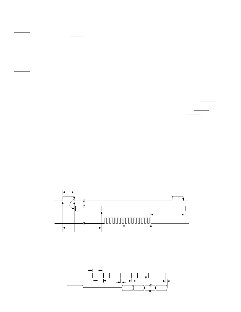
CONVST
BUSY
SCLK
SERIAL READ
OPERATION
CONVERSION
ENDS
9.8μs LATER
READ OPERATION
SHOULD END 300ns
PRIOR TO NEXT
FALLING EDGE OF
CONVST
OUTPUT
SERIAL
SHIFT
REGISTER
IS RESET
PART
WAKES
UP
CONVERSION
IS INITIATED
TRACK/HOLD
GOES INTO
HOLD
t
1
= 6μs
WAKE-UP
TIME
t
1
t
CONVERT
= 9.8μs
300ns MIN
Figure 4. Mode 2 Timing Diagram Where Automatic Sleep Function Is Initiated
t
2
4 LEADING ZEROS
DOUT (O/P)
SCLK (I/P)
t
6
1
2
3
4
5
6
15
16
DB0
DB10
DB11
3-STATE
t
5
t
3
t
4
3-STATE
t
2
=
t
3
= 35ns MIN,
t
4
= 60ns MAX,
t
5
= 10ns MIN,
t
6
= 50ns MAX @ 5V, A, B, VERSIONS
Figure 5. Data Read Operation
相關PDF資料 |
PDF描述 |
|---|---|
| AD7895BR-2 | 5 V, 12-Bit, Serial 3.8 ms ADC in 8-Pin Package |
| AD7896JR | 2.7 V to 5.5 V, 12-Bit, 8 us ADC in 8-Pin SO/DIP |
| AD7896 | 2.7 V to 5.5 V, 12-Bit, 8 us ADC in 8-Pin SO/DIP |
| AD7896AN | 14-Bit 50 kSPS ADC Ser. Out, 1.8V Operation 8-MSOP |
| AD7896AR | 2.7 V to 5.5 V, 12-Bit, 8 us ADC in 8-Pin SO/DIP |
相關代理商/技術參數 |
參數描述 |
|---|---|
| AD7895BR-10REEL | 制造商:Analog Devices 功能描述:ADC Single SAR 192ksps 12-bit Serial 8-Pin SOIC N T/R |
| AD7895BR-2 | 制造商:Analog Devices 功能描述:ADC Single SAR 192ksps 12-bit Serial 8-Pin SOIC N 制造商:Analog Devices 功能描述:ADC SGL SAR 192KSPS 12-BIT SERL 8SOIC N - Rail/Tube 制造商:Rochester Electronics LLC 功能描述:SERIAL 12 BIT BIPOLAR ADC I.C. - Bulk |
| AD7895BR-2REEL | 制造商:Analog Devices 功能描述:ADC Single SAR 192ksps 12-bit Serial 8-Pin SOIC N T/R |
| AD7895BRZ-10 | 功能描述:IC ADC 12BIT SRL 5V 8SOIC RoHS:是 類別:集成電路 (IC) >> 數據采集 - 模數轉換器 系列:- 其它有關文件:TSA1204 View All Specifications 標準包裝:1 系列:- 位數:12 采樣率(每秒):20M 數據接口:并聯 轉換器數目:2 功率耗散(最大):155mW 電壓電源:模擬和數字 工作溫度:-40°C ~ 85°C 安裝類型:表面貼裝 封裝/外殼:48-TQFP 供應商設備封裝:48-TQFP(7x7) 包裝:Digi-Reel® 輸入數目和類型:4 個單端,單極;2 個差分,單極 產品目錄頁面:1156 (CN2011-ZH PDF) 其它名稱:497-5435-6 |
| AD7895BRZ-10REEL | 功能描述:IC ADC 12BIT SRL 5V 8SOIC RoHS:是 類別:集成電路 (IC) >> 數據采集 - 模數轉換器 系列:- 產品培訓模塊:Lead (SnPb) Finish for COTS Obsolescence Mitigation Program 標準包裝:2,500 系列:- 位數:12 采樣率(每秒):3M 數據接口:- 轉換器數目:- 功率耗散(最大):- 電壓電源:- 工作溫度:- 安裝類型:表面貼裝 封裝/外殼:SOT-23-6 供應商設備封裝:SOT-23-6 包裝:帶卷 (TR) 輸入數目和類型:- |
發布緊急采購,3分鐘左右您將得到回復。