- 您現在的位置:買賣IC網 > PDF目錄373925 > AD7896 (Analog Devices, Inc.) 2.7 V to 5.5 V, 12-Bit, 8 us ADC in 8-Pin SO/DIP PDF資料下載
參數資料
| 型號: | AD7896 |
| 廠商: | Analog Devices, Inc. |
| 英文描述: | 2.7 V to 5.5 V, 12-Bit, 8 us ADC in 8-Pin SO/DIP |
| 中文描述: | 2.7 V至5.5 V,12位,8我們ADC的8引腳SO /文憑 |
| 文件頁數: | 10/12頁 |
| 文件大小: | 367K |
| 代理商: | AD7896 |
REV. B
–10–
AD7896
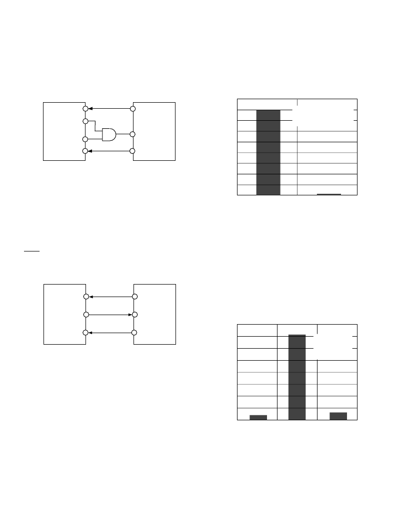
Figure 9 shows a histogram plot for 8192 conversions of a dc in-
put using the AD7896 with 3.3 V supply. The analog input was
set at the center of a code transition. It can be seen that almost
all the codes appear in the one output bin indicating very good
noise performance from the ADC. The rms noise performance
for the AD7896 for the plot below was 111
μ
V.
9000
0
2000
1000
3000
4000
5000
6000
7000
8000
1005
1006
CODE
F
SAMPLE
= 95kHz,
F
= 8.33 MHz,
AIN CENTERED ON CODE 1005,
rms NOISE = 0.138LSBS
O
Figure 9. Histogram of 8192 Conversions of a DC Input
The same data is presented in Figure 10 as in Figure 9 except
that in this case the output data read for the device occurs dur-
ing conversion. This has the effect of injecting noise onto the
die while bit decisions are being made and this increases the
noise generated by the AD7896. The histogram plot for 8192
conversions of the same dc input now shows a larger spread of
codes with the rms noise for the AD7896 increasing to 279
μ
V .
This effect will vary depending on where the serial clock edges
appear with respect to the bit trials of the conversion process. It
is possible to achieve the same level of performance when read-
ing during conversion as when reading after conversion depend-
ing on the relationship of the serial clock edges to the bit trial
points.
8000
0
2000
1000
1004
4000
3000
5000
6000
7000
1005
1006
CODE
O
F
SAMPLE
= 95 kHz,
F
= 8.33MHz,
AIN CENTERED ON
CODE 1005, rms
NOISE = 0.346 LSBS
Figure 10. Histogram of 8192 Conversions with Read
During Conversion
Another alternative scheme is to configure the ADSP-2103/
ADSP-2105 such that it accepts an external noncontinuous se-
rial clock. In this case, an external noncontinuous serial clock is
provided which drives the serial clock inputs of both the ADSP-
2103/ADSP-2105 and the AD7896. In this scheme, the serial
clock frequency is limited to 10 MHz by the AD7896.
AD7896
SDATA
SCLK
BUSY
SCLK1
DR1
ADSP-2103/5
IRQ2
RFS1
Figure 7. AD7896 to ADSP-2103 /5 Interface
AD7896–DSP56002/L002 Interface
Figure 8 shows an interface circuit between the AD7896 and the
DSP56002/L002 DSP processor. The DSP56002/L002 is con-
figured for normal mode asynchronous operation with gated
clock. It is also set up for a 16-bit word with SCK as gated
clock output. In this mode, the DSP56002/L002 provides six-
teen serial clock pulses to the AD7896 in a serial read operation.
The DSP56002/L002 assumes valid data on the first falling edge
of SCK so the interface is simply two-wire as shown in Figure 8.
The BUSY line from the AD7896 is connected to the MODA/
IRQA
input of the DSP56002/L002 so that an interrupt will be
generated at the end of conversion. This ensures that the read
operation will take place after conversion is finished.
AD7896
SDATA
SCLK
BUSY
SCK
SDR
DSP56002/L002
MODA /
IRQA
Figure 8. AD7896 to DSP56002/L002 Interface
AD7896 PERFORMANCE
Linearity
The linearity of the AD7896 is determined by the on-chip 12-
bit D/A converter. This is a segmented DAC which is laser
trimmed for 12-bit integral linearity and differential linearity.
Typical relative accuracy numbers for the part are
±
1/4 LSB
while the typical DNL errors are
±
1/2 LSB.
Noise
In an A/D converter, noise exhibits itself as code uncertainty in
dc applications and as the noise floor (in an FFT, for example)
in ac applications. In a sampling A/D converter like the
AD7896, all information about the analog input appears in the
baseband from dc to 1/2 the sampling frequency. The input
bandwidth of the track/hold exceeds the Nyquist bandwidth
and, therefore, an antialiasing filter should be used to remove
unwanted signals above f
S
/2 in the input signal in applications
where such signals exist.
相關PDF資料 |
PDF描述 |
|---|---|
| AD7896AN | 14-Bit 50 kSPS ADC Ser. Out, 1.8V Operation 8-MSOP |
| AD7896AR | 2.7 V to 5.5 V, 12-Bit, 8 us ADC in 8-Pin SO/DIP |
| AD7896BN | 2.7 V to 5.5 V, 12-Bit, 8 us ADC in 8-Pin SO/DIP |
| AD7896BR | 2.7 V to 5.5 V, 12-Bit, 8 us ADC in 8-Pin SO/DIP |
| AD7896SQ | 2.7 V to 5.5 V, 12-Bit, 8 us ADC in 8-Pin SO/DIP |
相關代理商/技術參數 |
參數描述 |
|---|---|
| AD7896AN | 功能描述:IC ADC 12BIT SRL T/H HS 8-DIP RoHS:否 類別:集成電路 (IC) >> 數據采集 - 模數轉換器 系列:- 產品培訓模塊:Lead (SnPb) Finish for COTS Obsolescence Mitigation Program 標準包裝:2,500 系列:- 位數:12 采樣率(每秒):3M 數據接口:- 轉換器數目:- 功率耗散(最大):- 電壓電源:- 工作溫度:- 安裝類型:表面貼裝 封裝/外殼:SOT-23-6 供應商設備封裝:SOT-23-6 包裝:帶卷 (TR) 輸入數目和類型:- |
| AD7896ANZ | 功能描述:IC ADC 12BIT SRL T/H HS 8DIP RoHS:是 類別:集成電路 (IC) >> 數據采集 - 模數轉換器 系列:- 標準包裝:1,000 系列:- 位數:12 采樣率(每秒):300k 數據接口:并聯 轉換器數目:1 功率耗散(最大):75mW 電壓電源:單電源 工作溫度:0°C ~ 70°C 安裝類型:表面貼裝 封裝/外殼:24-SOIC(0.295",7.50mm 寬) 供應商設備封裝:24-SOIC 包裝:帶卷 (TR) 輸入數目和類型:1 個單端,單極;1 個單端,雙極 |
| AD7896AR | 功能描述:IC ADC 12BIT SRL T/H HS 8-SOIC RoHS:否 類別:集成電路 (IC) >> 數據采集 - 模數轉換器 系列:- 標準包裝:1,000 系列:- 位數:12 采樣率(每秒):300k 數據接口:并聯 轉換器數目:1 功率耗散(最大):75mW 電壓電源:單電源 工作溫度:0°C ~ 70°C 安裝類型:表面貼裝 封裝/外殼:24-SOIC(0.295",7.50mm 寬) 供應商設備封裝:24-SOIC 包裝:帶卷 (TR) 輸入數目和類型:1 個單端,單極;1 個單端,雙極 |
| AD7896AR-REEL | 功能描述:IC ADC 12BIT SRL T/H HS 8-SOIC RoHS:否 類別:集成電路 (IC) >> 數據采集 - 模數轉換器 系列:- 標準包裝:1,000 系列:- 位數:12 采樣率(每秒):300k 數據接口:并聯 轉換器數目:1 功率耗散(最大):75mW 電壓電源:單電源 工作溫度:0°C ~ 70°C 安裝類型:表面貼裝 封裝/外殼:24-SOIC(0.295",7.50mm 寬) 供應商設備封裝:24-SOIC 包裝:帶卷 (TR) 輸入數目和類型:1 個單端,單極;1 個單端,雙極 |
| AD7896AR-REEL7 | 制造商:Rochester Electronics LLC 功能描述:- Tape and Reel |
發布緊急采購,3分鐘左右您將得到回復。