- 您現(xiàn)在的位置:買賣IC網(wǎng) > PDF目錄373925 > AD7898 (Analog Devices, Inc.) 5 V, 12-Bit, Serial 220 kSPS ADC in an 8-Lead Package PDF資料下載
參數(shù)資料
| 型號(hào): | AD7898 |
| 廠商: | Analog Devices, Inc. |
| 英文描述: | 5 V, 12-Bit, Serial 220 kSPS ADC in an 8-Lead Package |
| 中文描述: | 5伏,12位,220 kSPS的串行ADC的8引腳封裝 |
| 文件頁數(shù): | 8/16頁 |
| 文件大小: | 184K |
| 代理商: | AD7898 |
AD7898
–8–
REV. 0
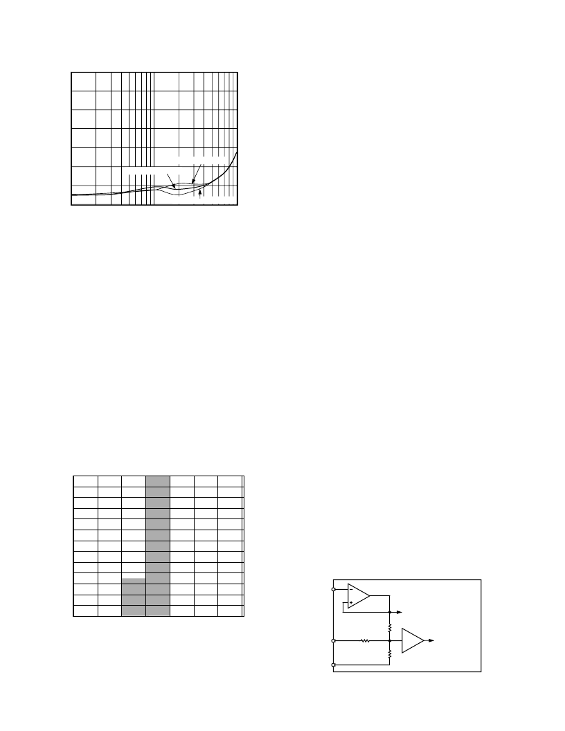
INPUT FREQUENCY
–
kHz
S
–
–
50
–
55
–
65
–
75
1000
100
10
–
40
–
45
–
60
–
70
V
DD
= V
DRIVE
= 5.25V
V
DD
= 5.0V, V
DRIVE
= 3.0V
V
DD
= V
DRIVE
= 4.75V
TPC 5. SINAD vs. Input Frequency at 220 kSPS
TPC 5 shows a graph of Signal to (Noise + Distortion)
ratio versus Input Frequency for various supply voltages
while sampling at 220 kSPS. The on-chip track-and-hold
can accommodate frequencies up to 4.7 MHz for AD7898-3,
and up to 3.6 MHz for AD7898-10, making the AD7898 ideal
for subsampling applications.
Noise
In an A/D converter, noise exhibits itself as a code uncertainty
in dc applications, and as the noise floor (in an FFT, for
example) in ac applications. In a sampling A/D converter like
the AD7898, all information about the analog input appears in
the baseband, from dc to half the sampling frequency. The input
bandwidth of the track/hold exceeds the Nyquist bandwidth
and, therefore, an antialiasing filter should be used to remove
unwanted signals above f
S
/2 in the input signal in applications
where such signals exist.
TPC 6 shows a histogram plot for 8192 conversions of a dc
input using the AD7898. The analog input was set at the center
of a code transition. It can be seen that almost all the codes
appear in one output bin, indicating very good noise perfor-
mance from the ADC.
5000
4000
2000
0
2044
2050
6000
3000
1000
5500
4500
2500
500
3500
1500
2049
2048
2047
2046
2045
6500
TPC 6. Histogram of 8192 Conversions of a DC Input
CONVERTER DETAILS
The AD7898 is a fast, 12-bit single supply A/D converter. It
provides the user with signal scaling, track/hold, A/D converter,
and serial interface logic functions on a single chip. The A/D
converter section of the AD7898 consists of a conventional
successive-approximation converter based around an R-2R
ladder structure. The signal scaling on the AD7898-10 and
AD7898-3 allows the part to handle
±
10 V and
±
2.5 V input
signals, respectively, while operating from a single 5V supply.
The part requires an external 2.5 V reference. The reference
input to the part is buffered on-chip. The AD7898 has two
operating modes, an internal clocking mode using an on-chip
oscillator and an external clocking mode using the SCLK as
the master clock. The latter mode features a power-down
mechanism. These modes are discussed in more detail in the
Operating Modes section.
A major advantage of the AD7898 is that it provides all of the
above functions in an 8-lead SOIC package. This offers the user
considerable spacing saving advantages over alternative solutions.
The AD7898 consumes only 22.5 mW maximum, making it
ideal for battery-powered applications.
In Mode 0 operation, conversion is initiated on the AD7898 by
pulsing the
CONVST
input. On the falling edge of
CONVST
,
the on-chip track/hold goes from track to hold mode, and the
conversion sequence is started. The conversion clock for the
part is generated internally using a laser-trimmed clock oscilla-
tor circuit. Conversion time for the AD7898 is 3.3
μ
s, and the
quiet time is 0.1
μ
s. To obtain optimum performance from the
part in Mode 0, the read operation should not occur during the
conversion.
In Mode 1 operation, conversion is initiated on the AD7898 by
the falling edge of
CS
. Sixteen SCLK cycles are required to
complete the conversion and access the conversion result, after
which time
CS
may be brought high. The internal oscillator is
not used as the conversion clock in this mode as the SCLK is
used instead. The maximum SCLK frequency is 3.7 MHz in
Mode 1 providing a minimum conversion time of 4.33
μ
s. As in
Mode 0, another conversion should not be initiated during the
quiet time after the end of conversion.
Both of these modes of operation allow the part to operate
at throughput rates up to 220 kHz and achieve data sheet
specifications.
CIRCUIT DESCRIPTION
Analog Input Section
The AD7898 is offered as two part types: the AD7898-10,
which handles a
±
10 V input voltage range; the AD7898-3,
which handles input voltage range
±
2.5 V.
V
IN
AGND
VREF
TO INTERNAL
COMPARATOR
TRACK/HOLD
TO ADC
REFERENCE
CIRCUITRY
R2
R3
R1
AD7898-10/AD7898-3
Figure 2. Analog Input Structure
相關(guān)PDF資料 |
PDF描述 |
|---|---|
| AD7898AR-10 | 5 V, 12-Bit, Serial 220 kSPS ADC in an 8-Lead Package |
| AD7898AR-3 | 5 V, 12-Bit, Serial 220 kSPS ADC in an 8-Lead Package |
| AD7899 | Evaluation Board for 5V, 12-Bit, Serial 220kSPS ADC in 8-Pin Package |
| AD7904 | 4-Channel, 1 MSPS, 8-/10-/12-Bit ADCs with Sequencer in 16-Lead TSSOP |
| AD7904BRU | 4-Channel, 1 MSPS, 8-/10-/12-Bit ADCs with Sequencer in 16-Lead TSSOP |
相關(guān)代理商/技術(shù)參數(shù) |
參數(shù)描述 |
|---|---|
| AD7898AR10 | 制造商:AD 功能描述:New |
| AD7898AR-10 | 功能描述:IC ADC 12BIT SRL HS 5V 8-SOIC RoHS:否 類別:集成電路 (IC) >> 數(shù)據(jù)采集 - 模數(shù)轉(zhuǎn)換器 系列:- 標(biāo)準(zhǔn)包裝:1,000 系列:- 位數(shù):12 采樣率(每秒):300k 數(shù)據(jù)接口:并聯(lián) 轉(zhuǎn)換器數(shù)目:1 功率耗散(最大):75mW 電壓電源:單電源 工作溫度:0°C ~ 70°C 安裝類型:表面貼裝 封裝/外殼:24-SOIC(0.295",7.50mm 寬) 供應(yīng)商設(shè)備封裝:24-SOIC 包裝:帶卷 (TR) 輸入數(shù)目和類型:1 個(gè)單端,單極;1 個(gè)單端,雙極 |
| AD7898AR-10 | 制造商:Analog Devices 功能描述:A/D CONVERTER (A-D) IC ((NW)) |
| AD7898AR-10REEL | 制造商:Analog Devices 功能描述:ADC Single SAR 220ksps 12-bit Serial 8-Pin SOIC N T/R 制造商:Rochester Electronics LLC 功能描述:5V 12-BIT SERIAL ADC IN 8-PIN PKG I.C. - Tape and Reel |
| AD7898AR-10REEL7 | 功能描述:IC ADC 12BIT SRL HS 5V 8-SOIC RoHS:否 類別:集成電路 (IC) >> 數(shù)據(jù)采集 - 模數(shù)轉(zhuǎn)換器 系列:- 標(biāo)準(zhǔn)包裝:1,000 系列:- 位數(shù):16 采樣率(每秒):45k 數(shù)據(jù)接口:串行 轉(zhuǎn)換器數(shù)目:2 功率耗散(最大):315mW 電壓電源:模擬和數(shù)字 工作溫度:0°C ~ 70°C 安裝類型:表面貼裝 封裝/外殼:28-SOIC(0.295",7.50mm 寬) 供應(yīng)商設(shè)備封裝:28-SOIC W 包裝:帶卷 (TR) 輸入數(shù)目和類型:2 個(gè)單端,單極 |
發(fā)布緊急采購,3分鐘左右您將得到回復(fù)。