- 您現在的位置:買賣IC網 > PDF目錄373925 > AD7908 (Analog Devices, Inc.) 8-Channel, 1 MSPS, 8-/10-/12-Bit ADCs with Sequencer in 20-Lead TSSOP PDF資料下載
參數資料
| 型號: | AD7908 |
| 廠商: | Analog Devices, Inc. |
| 英文描述: | 8-Channel, 1 MSPS, 8-/10-/12-Bit ADCs with Sequencer in 20-Lead TSSOP |
| 中文描述: | 8通道,1 MSPS的,8-/10-/12-Bit與序列ADC的20引腳TSSOP封裝 |
| 文件頁數: | 15/24頁 |
| 文件大小: | 607K |
| 代理商: | AD7908 |
AD7908/AD7918/AD7928
REV. A
Table V. SHADOW Register Bit Functions
MSB
V
IN
0
LSB
V
IN
7
V
IN
1
V
IN
2
V
IN
3
V
IN
4
V
IN
5
V
IN
6
V
IN
7
V
IN
0
V
IN
1
V
IN
2
V
IN
3
V
IN
4
V
IN
5
V
IN
6
------------------SEQUENCE ONE-------------------------------------------------------SEQUENCE TWO-----------------------
POWER-ON
DUMMY CONVERSION
DIN = ALL 1s
DIN: WRITE TO CONTROL REGISTER,
WRITE BIT = 1,
SELECT CODING, RANGE, AND POWER MODE.
SELECT CHANNEL A2–A0 FOR CONVERSION.
SEQ = SHADOW = 0
DOUT: CONVERSION RESULT FROM PREVIOUSLY
SELECTED CHANNEL A2–A0.
DIN: WRITE TO CONTROL REGISTER,
WRITE BIT = 1,
SELECT CODING, RANGE, AND POWER MODE.
SELECT A2–A0 FOR CONVERSION.
SEQ = SHADOW = 0
WRITE BIT = 1,
SEQ = SHADOW = 0
CS
CS
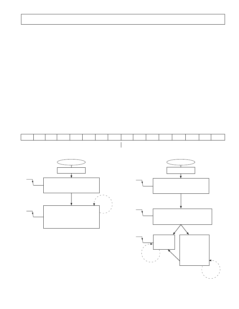
Figure 2. SEQ Bit = 0, SHADOW Bit = 0 Flowchart
SHADOW REGISTER
The SHADOW Register on the AD7908/AD7918/AD7928 is a
16-bit, write-only register. Data is loaded from the DIN pin of
the AD7908/AD7918/AD7928 on the falling edge of SCLK.
The data is transferred on the DIN line at the same time that a
conversion result is read from the part. This requires 16 serial
clock falling edges for the data transfer. The information is
clocked into the SHADOW Register, provided that the SEQ
and SHADOW bits were set to 0,1, respectively, in the previous
write to the Control Register. MSB denotes the first bit in the
data stream. Each bit represents an analog input from Channel
0 to Channel 7. Through programming the SHADOW Register,
two sequences of channels may be selected, through which the
AD7908/AD7918/AD7928 will cycle with each consecutive
conversion after the write to the SHADOW Register. Sequence
One will be performed first and then Sequence Two.
If the user
does not wish to perform a second sequence option, then all 0s
must be written to the last 8 LSBs of the SHADOW Register.
To select a sequence of channels, the associated channel bit
must be set for each analog input. The AD7908/AD7918/
AD7928 will continuously cycle through the selected channels
in ascending order beginning with the lowest channel, until a
write operation occurs (i.e., the WRITE bit is set to 1) with the
SEQ and SHADOW bits configured in any way except 1,0.
(See Table IV.) The bit functions are outlined in Table V.
Figure 2 reflects the traditional operation of a multichannel
ADC, where each serial transfer selects the next channel for
conversion. In this mode of operation the Sequencer function is
not used.
Figure 3 shows how to program the AD7908/AD7918/AD7928
to continuously convert on a particular sequence of channels. To
exit this mode of operation and revert back to the traditional
mode of operation of a multichannel ADC (as outlined in
Figure 2), ensure that the WRITE bit = 1 and the SEQ =
SHADOW = 0 on the next serial transfer. Figure 4 shows how a
sequence of consecutive channels can be converted on without
having to program the SHADOW Register or write to the part
on each serial transfer. Again to exit this mode of operation and
revert back to the traditional mode of operation of a multichannel
ADC (as outlined in Figure 2), ensure the WRITE bit = 1 and
the SEQ = SHADOW = 0 on the next serial transfer.
CS
POWER-ON
DUMMY CONVERSION
DIN = ALL 1s
DIN: WRITE TO CONTROL REGISTER,
WRITE BIT = 1,
SELECT CODING, RANGE, AND POWER MODE.
SELECT CHANNEL A2–A0 FOR CONVERSION.
SEQ = 0 SHADOW = 1
DOUT: CONVERSION RESULT FROM PREVIOUSLY
SELECTED CHANNEL A2–A0.
DIN: WRITE TO SHADOW REGISTER, SELECTING
WHICH CHANNELS TO CONVERT ON; CHANNELS
SELECTED NEED NOT BE CONSECUTIVE CHANNELS
WRITE BIT = 1,
SEQ = 1,
SHADOW = 0
CS
CS
WRITE BIT = 0
WRITE BIT = 1
SEQ = 1 SHADOW = 0
CONTINUOUSLY
CONVERTS ON
THE SELECTED
SEQUENCE OF
CHANNELS
WRITE BIT = 0
WRITE BIT = 0
CONTINUOUSLY
CONVERTS ON THE
SELECTED SEQUENCE
OF CHANNELS BUT WILL
ALLOW RANGE, CODING,
AND SO ON, TO CHANGE
IN THE CONTROL
REGISTER WITHOUT
INTERRUPTING THE
SEQUENCE, PROVIDED
SEQ = 1 SHADOW = 0
Figure 3. SEQ Bit = 0, SHADOW Bit = 1 Flowchart
–15–
相關PDF資料 |
PDF描述 |
|---|---|
| AD7908BRU | 8-Channel, 1 MSPS, 8-/10-/12-Bit ADCs with Sequencer in 20-Lead TSSOP |
| AD7908BRU-REEL | 8-Channel, 1 MSPS, 8-/10-/12-Bit ADCs with Sequencer in 20-Lead TSSOP |
| AD7908BRU-REEL7 | 8-Channel, 1 MSPS, 8-/10-/12-Bit ADCs with Sequencer in 20-Lead TSSOP |
| AD7918 | 8-Channel, 1 MSPS, 8-/10-/12-Bit ADCs with Sequencer in 20-Lead TSSOP |
| AD7918BRU | 8-Channel, 1 MSPS, 8-/10-/12-Bit ADCs with Sequencer in 20-Lead TSSOP |
相關代理商/技術參數 |
參數描述 |
|---|---|
| AD7908BRU | 制造商:Analog Devices 功能描述:ADC Single SAR 1Msps 8-bit Serial 20-Pin TSSOP 制造商:Rochester Electronics LLC 功能描述:8-BIT 8, CH 1 MSPS ADC - Bulk 制造商:Analog Devices 功能描述:IC 8BIT ADC SMD 7908 TSSOP20 |
| AD7908BRU-REEL | 制造商:Analog Devices 功能描述:ADC Single SAR 1Msps 8-bit Serial 20-Pin TSSOP T/R 制造商:Analog Devices 功能描述:ADC SGL SAR 1MSPS 8BIT SERL 20TSSOP - Tape and Reel |
| AD7908BRU-REEL7 | 制造商:Analog Devices 功能描述:ADC Single SAR 1Msps 8-bit Serial 20-Pin TSSOP T/R 制造商:Analog Devices 功能描述:ADC SGL SAR 1MSPS 8BIT SERL 20TSSOP - Tape and Reel |
| AD7908BRUZ | 功能描述:IC ADC 8BIT 8CH 1MSPS 20-TSSOP RoHS:是 類別:集成電路 (IC) >> 數據采集 - 模數轉換器 系列:- 標準包裝:1 系列:microPOWER™ 位數:8 采樣率(每秒):1M 數據接口:串行,SPI? 轉換器數目:1 功率耗散(最大):- 電壓電源:模擬和數字 工作溫度:-40°C ~ 125°C 安裝類型:表面貼裝 封裝/外殼:24-VFQFN 裸露焊盤 供應商設備封裝:24-VQFN 裸露焊盤(4x4) 包裝:Digi-Reel® 輸入數目和類型:8 個單端,單極 產品目錄頁面:892 (CN2011-ZH PDF) 其它名稱:296-25851-6 |
| AD7908BRUZ | 制造商:Analog Devices 功能描述:IC 8BIT ADC SMD 7908 TSSOP20 |
發布緊急采購,3分鐘左右您將得到回復。