- 您現在的位置:買賣IC網 > PDF目錄373926 > AD790JR-REEL7 (ANALOG DEVICES INC) Fast, Precision Comparator PDF資料下載
參數資料
| 型號: | AD790JR-REEL7 |
| 廠商: | ANALOG DEVICES INC |
| 元件分類: | 運動控制電子 |
| 英文描述: | Fast, Precision Comparator |
| 中文描述: | COMPARATOR, 1500 uV OFFSET-MAX, 45 ns RESPONSE TIME, PDSO8 |
| 封裝: | SOIC-8 |
| 文件頁數: | 6/8頁 |
| 文件大小: | 211K |
| 代理商: | AD790JR-REEL7 |
AD790
REV. B
–6–
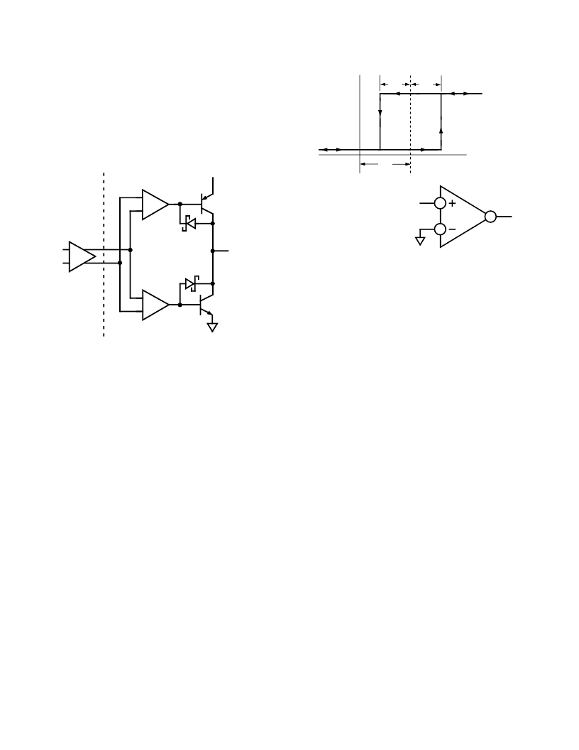
CIRCUIT DE SCRIPT ION
T he AD790 possesses the overall characteristics of a standard
monolithic comparator: differential inputs, high gain and a logic
output. However, its function is implemented with an architec-
ture which offers several advantages over previous comparator
designs. Specifically, the output stage alleviates some of the limi-
tations of classic “T T L” comparators and provides a symmetric
output. A simplified representation of the AD790 circuitry is
shown in Figure 13.
A1
A2
Av
OUTPUT
GAIN STAGE
OUTPUT STAGE
Q2
Q1
–
+
–
+
–
+
IN
+
IN
–
V
LOGIC
GND
Figure 13. AD790 Block Diagram
T he output stage takes the amplified differential input signal and
converts it to a single-ended logic output. T he output swing is
defined by the pull-up PNP and the pull-down NPN. T hese pro-
duce inherent rail-to-rail output levels, compatible with CMOS
logic, as well as T T L, without the need for clamping to internal
bias levels. Furthermore, the pull-up and pull-down levels are
symmetric about the center of the supply range and are refer-
enced off the V
LOGIC
supply and ground. T he output stage has
nearly symmetric dynamic drive capability, yielding equal rise
and fall times into subsequent logic gates.
Unlike classic T T L or CMOS output stages, the AD790 circuit
does not exhibit large current spikes due to unwanted current
flow between the output transistors. T he AD790 output stage
has a controlled switching scheme in which amplifiers A1 and
A2 drive the output transistors in a manner designed to reduce
the current flow between Q1 and Q2. T his also helps minimize
the disturbances feeding back to the input which can cause
troublesome oscillations.
T he output high and low levels are well controlled values de-
fined by V
LOGIC
(+5 V), ground and the transistor equivalent
“Schottky” clamps and are compatible with T T L and CMOS
logic requirements. T he fanout of the output stage is shown in
Figure 6 for standard LST T L or HCMOS gates. Output drive
behavior vs. capacitive load is shown in Figure 5.
HY ST E RE SIS
T he AD790 uses internal feedback to develop hysteresis about
the input reference voltage. Figure 14 shows how the input off-
set voltage and hysteresis terms are defined. Input offset voltage
(V
OS
) is the difference between the center of the hysteresis
range and the ground level. T his can be either positive or nega-
tive. T he hysteresis voltage (V
H
) is one-half the width of the
V
OH
V
OL
H
V
= HYSTERESIS VOLTAGE
H
V
0
H
V
V
OUT
IN
+
V
OS
V
OS
= INPUT OFFSET VOLTAGE
2
3
7
IN
+
OUT
V
GND
Figure 14. Hysteresis Definitions (N, Q Package Pinout)
hysteresis range. T his built-in hysteresis allows the AD790 to
avoid oscillation when an input signal slowly crosses the ground
level.
SUPPLY VOLT AGE CONNE CT IONS
T he AD790 may be operated from either single or dual supply
voltages. Internally, the V
LOGIC
circuitry and the analog front-
end of the AD790 are connected to separate supply pins. If dual
supplies are used, any combination of voltages in which +V
S
≥
V
LOGIC
– 0.5 V and –V
S
≤
0 may be chosen. For single supply
operation (i.e., +V
S
= V
LOGIC
), the supply voltage can be oper-
ated between 4.5 V and 7 V. Figure 15 shows some other ex-
amples of typical supply connections possible with the AD790.
BY PASSING AND GROUNDING
Although the AD790 is designed to be stable and free from os-
cillations, it is important to properly bypass and ground the
power supplies. Ceramic 0.1
μ
F capacitors are recommended
and should be connected directly at the AD790’s supply pins.
T hese capacitors provide transient currents to the device during
comparator switching. T he AD790 has three supply voltage
pins, +V
S
, –V
S
and V
LOGIC
. It is important to have a common
ground lead on the board for the supply grounds and the GND
pin of the AD790 to provide the proper return path for the sup-
ply current.
LAT CH OPE RAT ION
T he AD790 has a latch function for retaining input information
at the output. T he comparator decision is “latched” and the
output state is held when Pin 5 is brought low. As long as Pin 5
is kept low, the output remains in the high or low state, and
does not respond to changing inputs. Proper capture of the in-
put signal requires that the timing relationships shown in Fig-
ure 12 are followed. Pin 5 should be driven with CMOS or
T T L logic levels.
T he output of the AD790 will respond to the input when Pin 5
is at a high logic level. When not in use, Pin 5 should be con-
nected to the positive logic supply. When using dual supplies, it
is recommended that a 510
resistor be placed in series with
Pin 5 and the driving logic gate to limit input currents during
power up.
相關PDF資料 |
PDF描述 |
|---|---|
| AD790 | Fast, Precision Comparator |
| AD790AQ | Fast, Precision Comparator |
| AD790BQ | Fast, Precision Comparator |
| AD790JN | Fast, Precision Comparator |
| AD790JR | Fast, Precision Comparator |
相關代理商/技術參數 |
參數描述 |
|---|---|
| AD790JRZ | 功能描述:IC COMPARATOR PREC W/LATCH 8SOIC RoHS:是 類別:集成電路 (IC) >> 線性 - 比較器 系列:- 標準包裝:1 系列:- 類型:通用 元件數:1 輸出類型:CMOS,開路集電極,TTL 電壓 - 電源,單路/雙路(±):2.7 V ~ 5.5 V 電壓 - 輸入偏移(最小值):7mV @ 5V 電流 - 輸入偏壓(最小值):0.25µA @ 5V 電流 - 輸出(標準):84mA @ 5V 電流 - 靜態(最大值):120µA CMRR, PSRR(標準):- 傳輸延遲(最大):600ns 磁滯:- 工作溫度:-40°C ~ 85°C 封裝/外殼:SC-74A,SOT-753 安裝類型:表面貼裝 包裝:剪切帶 (CT) 產品目錄頁面:1268 (CN2011-ZH PDF) 其它名稱:*LMV331M5*LMV331M5/NOPBLMV331M5CT |
| AD790JRZ-REEL | 功能描述:IC COMPARATOR PREC HS 8-SOIC RoHS:是 類別:集成電路 (IC) >> 線性 - 比較器 系列:- 產品培訓模塊:Lead (SnPb) Finish for COTS Obsolescence Mitigation Program 標準包裝:2,500 系列:- 類型:通用 元件數:1 輸出類型:CMOS,推挽式,滿擺幅,TTL 電壓 - 電源,單路/雙路(±):2.5 V ~ 5.5 V,±1.25 V ~ 2.75 V 電壓 - 輸入偏移(最小值):5mV @ 5.5V 電流 - 輸入偏壓(最小值):1pA @ 5.5V 電流 - 輸出(標準):- 電流 - 靜態(最大值):24µA CMRR, PSRR(標準):80dB CMRR,80dB PSRR 傳輸延遲(最大):450ns 磁滯:±3mV 工作溫度:-40°C ~ 85°C 封裝/外殼:6-WFBGA,CSPBGA 安裝類型:表面貼裝 包裝:管件 其它名稱:Q3554586 |
| AD790JRZ-REEL7 | 功能描述:IC COMPARATOR PREC W/LATCH 8SOIC RoHS:是 類別:集成電路 (IC) >> 線性 - 比較器 系列:- 產品培訓模塊:Lead (SnPb) Finish for COTS Obsolescence Mitigation Program 標準包裝:2,500 系列:- 類型:通用 元件數:1 輸出類型:CMOS,推挽式,滿擺幅,TTL 電壓 - 電源,單路/雙路(±):2.5 V ~ 5.5 V,±1.25 V ~ 2.75 V 電壓 - 輸入偏移(最小值):5mV @ 5.5V 電流 - 輸入偏壓(最小值):1pA @ 5.5V 電流 - 輸出(標準):- 電流 - 靜態(最大值):24µA CMRR, PSRR(標準):80dB CMRR,80dB PSRR 傳輸延遲(最大):450ns 磁滯:±3mV 工作溫度:-40°C ~ 85°C 封裝/外殼:6-WFBGA,CSPBGA 安裝類型:表面貼裝 包裝:管件 其它名稱:Q3554586 |
| AD790KN | 制造商:AD 制造商全稱:Analog Devices 功能描述:Fast, Precision Comparator |
| AD790S | 制造商:AD 制造商全稱:Analog Devices 功能描述:Fast, Precision Comparator |
發布緊急采購,3分鐘左右您將得到回復。