- 您現在的位置:買賣IC網 > PDF目錄373925 > AD7914 (Analog Devices, Inc.) 4-Channel, 1 MSPS, 8-/10-/12-Bit ADCs with Sequencer in 16-Lead TSSOP PDF資料下載
參數資料
| 型號: | AD7914 |
| 廠商: | Analog Devices, Inc. |
| 元件分類: | ADC |
| 英文描述: | 4-Channel, 1 MSPS, 8-/10-/12-Bit ADCs with Sequencer in 16-Lead TSSOP |
| 中文描述: | 4通道,1 MSPS的,8-/10-/12-Bit ADC的16與序列鉛TSSOP封裝 |
| 文件頁數: | 17/24頁 |
| 文件大小: | 411K |
| 代理商: | AD7914 |
AD7904/AD7914/AD7924
–17–
REV. 0
16-bit word. This 16-bit data stream consists of two leading
zeros, two address bits indicating which channel the conversion
result corresponds to, followed by the 12 bits of conversion data
for the AD7924 (10 bits of data for the AD7914 and 8 bits of data
for the AD7904, each followed by 2 and 4 trailing zeros, respec-
tively). For applications where power consumption is of concern,
the power-down modes should be used between conversions or
bursts of several conversions to improve power performance.
See the Modes of Operation section of the data sheet.
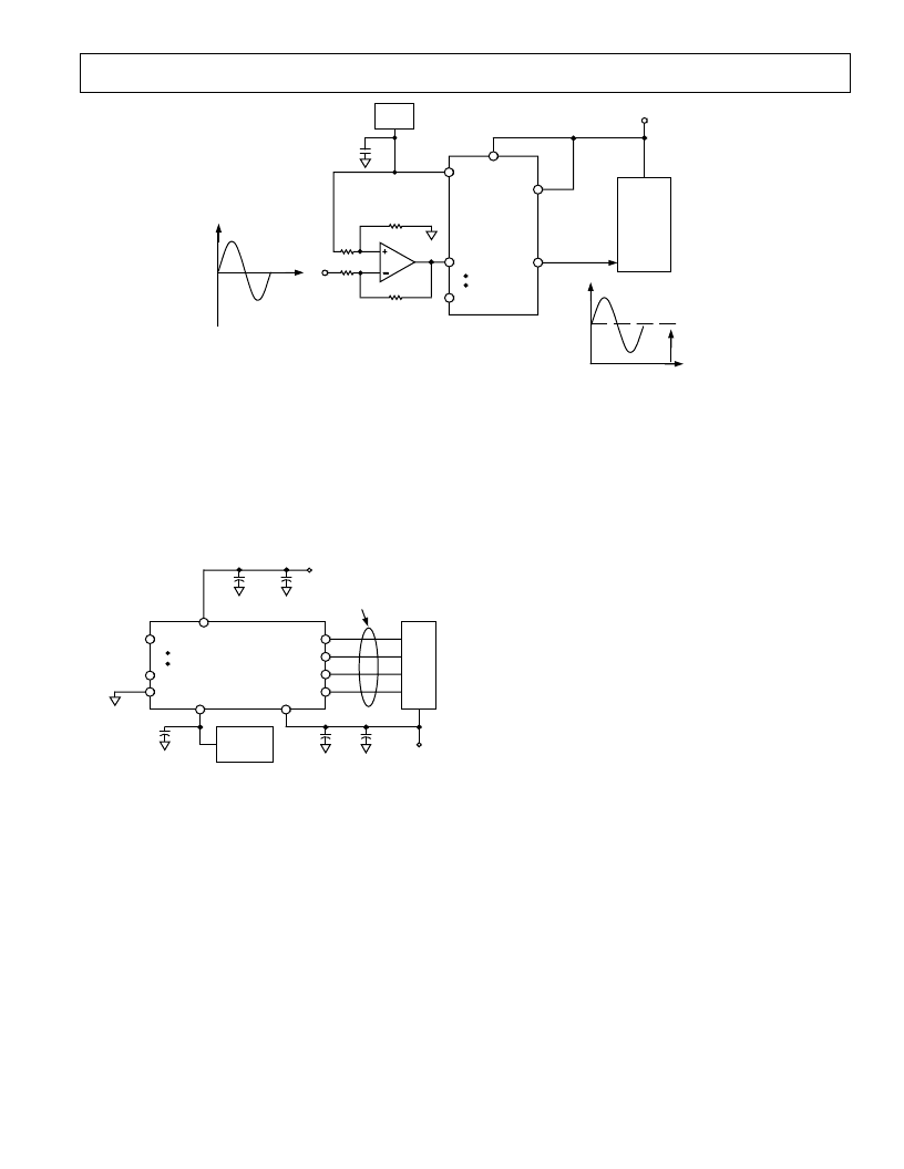
SERIAL
INTERFACE
AD780
2.5V
AD7904/
AD7914/
AD7924
0.1 F
C/ P
0.1 F
10 F
3V
SUPPLY
5V
SUPPLY
0.1 F
10 F
AGND
V
DD
V
IN
0
V
IN
3
0V TO REF
IN
SCLK
DOUT
CS
DIN
V
DRIVE
REF
IN
NOTE: ALL UNUSED INPUT CHANNELS SHOULD BE CONNECTED TO AGND
Figure 10. Typical Connection Diagram
Analog Input Selection
Any one of four analog input channels may be selected for con-
version by programming the multiplexer with the address bits
ADD1 and ADD0 in the Control Register. The channel con-
figurations are shown in Table II.
The AD7904/AD7914/AD7924 may also be configured to auto-
matically cycle through a number of channels as selected. The
sequencer feature is accessed via the SEQ1 and SEQ0 bits in the
Control Register, see Table IV. The AD7904/AD7914/AD7924
can be programmed to continuously convert on a number of
consecutive channels in ascending order from Channel 0 to a
selected final channel as determined by the channel address bits
ADD1 and ADD0. This is possible if the SEQ1 and SEQ0 bits
are set to 1,1. The next serial transfer will then act on the sequence
programmed by executing a conversion on Channel 0. The next
serial transfer will result in a conversion on Channel 1, and so
on, until the channel selected via the address bits ADD1, ADD0
is reached.
It is not necessary to write to the Control Register again once a
sequencer operation has been initiated. The WRITE bit must be
set to zero or the DIN line tied low to ensure the Control Regis-
ter is not accidently overwritten, or the sequence operation
interrupted. If the Control Register is written to at any time
during the sequence then it must be ensured that the SEQ1 and
SEQ0 bits are set to 1,0 to avoid interrupting the automatic
conversion sequence. This pattern will continue until such time
as the AD7904/AD7914/AD7924 is written to and the SEQ1
and SEQ0 bits are configured with any bit combination except
1,0 resulting in the termination of the sequence. If uninter-
rupted, however (WRITE bit = 0, or WRITE bit = 1 and SEQ1
and SEQ0 bits are set to 1,0), then upon completion of the
sequence, the AD7904/AD7914/AD7924 sequencer will return
to the Channel 0 and commence the sequence again.
Regardless of which channel selection method is used, the 16-bit
word output from the AD7924 during each conversion will always
contain two leading zeros, two channel address bits that the con-
version result corresponds to, followed by the 12-bit conversion
result; the AD7914 will output two leading zeros, two channel
address bits that the conversion result corresponds to, followed by
the 10-bit conversion result and two trailing zeros; the AD7904 will
output two leading zeros, two channel address bits that the conver-
sion result corresponds to, followed by the 8-bit conversion result
and four trailing zeros. See the Serial Interface section.
Digital Inputs
The digital inputs applied to the AD7904/AD7914/AD7924 are
not limited by the maximum ratings that limit the analog inputs.
Instead, the digital inputs applied can go to 7 V and are not
restricted by the V
DD
+ 0.3 V limit as on the analog inputs.
Another advantage of SCLK, DIN, and
CS
not being restricted
by the V
DD
+ 0.3 V limit is the fact that power supply sequenc-
ing issues are avoided. If
CS
, DIN, or SCLK are applied before
V
DD
there is no risk of latch-up as there would be on the analog
inputs if a signal greater than 0.3 V was applied prior to V
DD
.
V
DRIVE
The AD7904/AD7914/AD7924 also have the V
DRIVE
feature.
V
DRIVE
controls the voltage at which the serial interface oper-
ates. V
DRIVE
allows the ADC to easily interface to both 3 V and
5 V processors. For example, if the AD7904/AD7914/AD7924
were operated with a V
DD
of 5 V, the V
DRIVE
pin could be pow-
ered from a 3 V supply. The AD7904/AD7914/AD7924 have
R3
R2
R4
REF
IN
V
IN
0
V
IN
3
AD7904/
AD7914/
AD7924
DSP/ P
V
DD
0.1 F
V
V
DD
V
DRIVE
DOUT
TWOS
COMPLEMENT
+REF
IN
REF
IN
–REF
IN
011…111
000…000
100…000
(= 0V)
(= 2 REF
IN
)
0V
V
R1
R1 R2 R3 R4
V
DD
V
REF
Figure 9. Handling Bipolar Signals
相關PDF資料 |
PDF描述 |
|---|---|
| AD7914BRU | 4-Channel, 1 MSPS, 8-/10-/12-Bit ADCs with Sequencer in 16-Lead TSSOP |
| AD7924 | 4-Channel, 1 MSPS, 8-/10-/12-Bit ADCs with Sequencer in 16-Lead TSSOP |
| AD7924BRU | 4-Channel, 1 MSPS, 8-/10-/12-Bit ADCs with Sequencer in 16-Lead TSSOP |
| AD7908 | 8-Channel, 1 MSPS, 8-/10-/12-Bit ADCs with Sequencer in 20-Lead TSSOP |
| AD7908BRU | 8-Channel, 1 MSPS, 8-/10-/12-Bit ADCs with Sequencer in 20-Lead TSSOP |
相關代理商/技術參數 |
參數描述 |
|---|---|
| AD7914BRU | 制造商:Analog Devices 功能描述:ADC Single SAR 1Msps 10-bit Serial 16-Pin TSSOP 制造商:Analog Devices 功能描述:IC 10BIT ADC SMD 7914 TSSOP16 |
| AD7914BRU-REEL | 制造商:Analog Devices 功能描述:ADC Single SAR 1Msps 10-bit Serial 16-Pin TSSOP T/R 制造商:Analog Devices 功能描述:ADC SGL SAR 1MSPS 10-BIT SERL 16TSSOP - Tape and Reel 制造商:Rochester Electronics LLC 功能描述:10-BIT 4,CH 1 MSPS ADC I.C. - Tape and Reel |
| AD7914BRU-REEL7 | 制造商:Analog Devices 功能描述:ADC Single SAR 1Msps 10-bit Serial 16-Pin TSSOP T/R 制造商:Rochester Electronics LLC 功能描述:10-BIT 4,CH 1 MSPS ADC I.C. - Tape and Reel |
| AD7914BRUZ | 功能描述:IC ADC 10BIT 4CH 1MSPS 16TSSOP RoHS:是 類別:集成電路 (IC) >> 數據采集 - 模數轉換器 系列:- 標準包裝:1 系列:microPOWER™ 位數:8 采樣率(每秒):1M 數據接口:串行,SPI? 轉換器數目:1 功率耗散(最大):- 電壓電源:模擬和數字 工作溫度:-40°C ~ 125°C 安裝類型:表面貼裝 封裝/外殼:24-VFQFN 裸露焊盤 供應商設備封裝:24-VQFN 裸露焊盤(4x4) 包裝:Digi-Reel® 輸入數目和類型:8 個單端,單極 產品目錄頁面:892 (CN2011-ZH PDF) 其它名稱:296-25851-6 |
| AD7914BRUZ-REEL7 | 功能描述:IC ADC 10BIT 4CH W/SEQ 16TSSOP RoHS:是 類別:集成電路 (IC) >> 數據采集 - 模數轉換器 系列:- 標準包裝:2,500 系列:- 位數:16 采樣率(每秒):15 數據接口:MICROWIRE?,串行,SPI? 轉換器數目:1 功率耗散(最大):480µW 電壓電源:單電源 工作溫度:-40°C ~ 85°C 安裝類型:表面貼裝 封裝/外殼:38-WFQFN 裸露焊盤 供應商設備封裝:38-QFN(5x7) 包裝:帶卷 (TR) 輸入數目和類型:16 個單端,雙極;8 個差分,雙極 配用:DC1011A-C-ND - BOARD DELTA SIGMA ADC LTC2494 |
發布緊急采購,3分鐘左右您將得到回復。