- 您現在的位置:買賣IC網 > PDF目錄373925 > AD7928BRU-REEL (ANALOG DEVICES INC) 8-Channel, 1 MSPS, 8-/10-/12-Bit ADCs with Sequencer in 20-Lead TSSOP PDF資料下載
參數資料
| 型號: | AD7928BRU-REEL |
| 廠商: | ANALOG DEVICES INC |
| 元件分類: | ADC |
| 英文描述: | 8-Channel, 1 MSPS, 8-/10-/12-Bit ADCs with Sequencer in 20-Lead TSSOP |
| 中文描述: | 8-CH 12-BIT SUCCESSIVE APPROXIMATION ADC, SERIAL ACCESS, PDSO20 |
| 封裝: | MO-153AC, TSSOP-20 |
| 文件頁數: | 19/24頁 |
| 文件大小: | 607K |
| 代理商: | AD7928BRU-REEL |
AD7908/AD7918/AD7928
REV. A
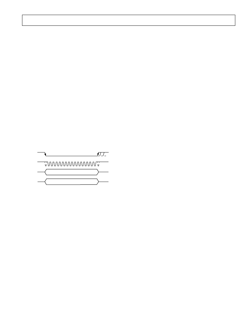
Normal Mode (PM1 = PM0 = 1)
This mode is intended for the fastest throughput rate performance
as the user does not have to worry about any power-up times
with the AD7908/AD7918/AD7928 remaining fully powered at
all times. Figure 12 shows the general diagram of the operation
of the AD7908/AD7918/AD7928 in this mode.
The conversion is initiated on the falling edge of
CS
and the
track-and-hold will enter hold mode as described in the Serial
Interface section. The data presented to the AD7908/AD7918/
AD7928 on the DIN line during the first 12 clock cycles of the
data transfer are loaded into the Control Register (provided
WRITE bit is set to 1). If data is to be written to the SHADOW
Register (SEQ = 0, SHADOW = 1 on previous write), data pre-
sented on the DIN line during the first 16 SCLK cycles is loaded
into the SHADOW Register. The part will remain fully powered
up in Normal mode at the end of the conversion as long as PM1
and PM0 are both loaded with 1 on every data transfer.
Sixteen serial clock cycles are required to complete the conversion
and access the conversion result. The track-and-hold will go back
into track on the 14th SCLK falling edge.
CS
may then idle high
until the next conversion or may idle low until sometime prior to
the next conversion, (effectively idling
CS
low).
Once a data transfer is complete (DOUT has returned to three-
state), another conversion can be initiated after the quiet time,
t
QUIET
,
has elapsed by bringing
CS
low again.
1
12
CS
SCLK
DOUT
DIN
16
1 LEADING ZERO + 3 CHANNEL IDENTIFIER BITS
+ CONVERSION RESULT
NOTES
1. CONTROL REGISTER DATA IS LOADED ON FIRST 12 SCLK CYCLES
2. SHADOW REGISTER DATA IS LOADED ON FIRST 16 SCLK CYCLES
DATA IN TO CONTROL/SHADOW REGISTER
Figure 12. Normal Mode Operation
Full Shutdown (PM1 = 1, PM0 = 0)
In this mode, all internal circuitry on the AD7908/AD7918/
AD7928 is powered down. The part retains information in the
Control Register during full shutdown. The AD7908/AD7918/
AD7928 remains in full shutdown until the power management
bits in the Control Register, PM1 and PM0, are changed.
If a write to the Control Register occurs while the part is in Full
Shutdown, with the power management bits changed to PM0 =
PM1 = 1, Normal mode, the part will begin to power up on the
CS
rising edge. The track-and-hold that was in hold while the
part was in Full Shutdown will return to track on the 14th SCLK
falling edge.
To ensure that the part is fully powered up, t
POWER UP
, should have
elapsed before the next
CS
falling edge. Figure 13 shows the
general diagram for this sequence.
Auto Shutdown (PM1 = 0, PM0 = 1)
In this mode, the AD7908/AD7918/AD7928 automatically
enters shutdown at the end of each conversion when the control
register is updated. When the part is in shutdown, the track and
hold is in hold mode. Figure 14 shows the general diagram of
the operation of the AD7908/AD7918/AD7928 in this mode. In
shutdown mode, all internal circuitry on the AD7908/AD7918/
AD7928 is powered down. The part retains information in the
Control Register during shutdown. The AD7908/AD7918/
AD7928 remains in shutdown until the next
CS
falling edge it
receives. On this
CS
falling edge, the track-and-hold that was in
hold while the part was in shutdown will return to track. Wake-
up time from auto shutdown is 1 μs, and the user should ensure
that 1 μs has elapsed before attempting a valid conversion.
When running the AD7908/AD7918/AD7928 with a 20 MHz
clock, one dummy cycle should be sufficient to ensure the part
is fully powered up. During this dummy cycle the contents of
the Control Register should remain unchanged; therefore the
WRITE bit should be 0 on the DIN line. This dummy cycle
effectively halves the throughput rate of the part, with every
other conversion result being valid. In this mode, the power
consumption of the part is greatly reduced with the part enter-
ing shutdown at the end of each conversion. When the Control
Register is programmed to move into Auto Shutdown, it does so
at the end of the conversion. The user can move the ADC in
and out of the low power state by controlling the
CS
signal.
Powering Up the AD7908/AD7918/AD7928
When supplies are first applied to the AD7908/AD7918/AD7928,
the ADC may power up in any of the operating modes of the
part. To ensure the part is placed into the required operating
mode, the user should perform a dummy cycle operation as out-
lined in Figure 15.
The three dummy conversion operation outlined in Figure 15
must be performed to place the part into the Auto Shutdown
mode. The first two conversions of this dummy cycle operation
are performed with the DIN line tied high; for the third conver-
sion of the dummy cycle operation, the user should write the
desired Control Register configuration to the AD7908/AD7918/
AD7928 in order to place the part into the Auto Shutdown
mode. On the third
CS
rising edge after the supplies are applied,
the Control Register will contain the correct information and
valid data will result from the next conversion.
Therefore, to ensure the part is placed into the correct operating
mode, when supplies are first applied to the AD7908/AD7918/
AD7928, the user must first issue two serial write operations
with the DIN line tied high, and on the third conversion cycle the
user can then write to the Control Register to place the part into
any of the operating modes. The user should not write to the
SHADOW Register until the fourth conversion cycle after the
supplies are applied to the ADC, in order to guarantee the
Control Register contains the correct data.
If the user wants to place the part into either the Normal mode
or Full Shutdown mode, the second dummy cycle with DIN tied
high can be omitted from the three dummy conversion operation
outlined in Figure 15.
–19–
相關PDF資料 |
PDF描述 |
|---|---|
| AD7928BRU-REEL7 | 8-Channel, 1 MSPS, 8-/10-/12-Bit ADCs with Sequencer in 20-Lead TSSOP |
| AD790JR-REEL | Fast, Precision Comparator |
| AD790JR-REEL7 | Fast, Precision Comparator |
| AD790 | Fast, Precision Comparator |
| AD790AQ | Fast, Precision Comparator |
相關代理商/技術參數 |
參數描述 |
|---|---|
| AD7928BRU-REEL7 | 制造商:Analog Devices 功能描述:ADC Single SAR 1Msps 12-bit Serial 20-Pin TSSOP T/R 制造商:Rochester Electronics LLC 功能描述:12-BIT 8, CH 1 MSPS ADC I.C. - Tape and Reel |
| AD7928BRUZ | 功能描述:IC ADC 12BIT 8CH 1MSPS 20-TSSOP RoHS:是 類別:集成電路 (IC) >> 數據采集 - 模數轉換器 系列:- 標準包裝:1 系列:microPOWER™ 位數:8 采樣率(每秒):1M 數據接口:串行,SPI? 轉換器數目:1 功率耗散(最大):- 電壓電源:模擬和數字 工作溫度:-40°C ~ 125°C 安裝類型:表面貼裝 封裝/外殼:24-VFQFN 裸露焊盤 供應商設備封裝:24-VQFN 裸露焊盤(4x4) 包裝:Digi-Reel® 輸入數目和類型:8 個單端,單極 產品目錄頁面:892 (CN2011-ZH PDF) 其它名稱:296-25851-6 |
| AD7928BRUZ | 制造商:Analog Devices 功能描述:IC 12BIT ADC SMD 7928 TSSOP8 |
| AD7928BRUZ-REEL | 功能描述:IC ADC 12BIT 8CH W/SEQ 20TSSOP RoHS:是 類別:集成電路 (IC) >> 數據采集 - 模數轉換器 系列:- 標準包裝:1,000 系列:- 位數:16 采樣率(每秒):45k 數據接口:串行 轉換器數目:2 功率耗散(最大):315mW 電壓電源:模擬和數字 工作溫度:0°C ~ 70°C 安裝類型:表面貼裝 封裝/外殼:28-SOIC(0.295",7.50mm 寬) 供應商設備封裝:28-SOIC W 包裝:帶卷 (TR) 輸入數目和類型:2 個單端,單極 |
| AD7928BRUZ-REEL7 | 功能描述:IC ADC 12BIT 8CH W/SEQ 20TSSOP RoHS:是 類別:集成電路 (IC) >> 數據采集 - 模數轉換器 系列:- 標準包裝:1,000 系列:- 位數:16 采樣率(每秒):45k 數據接口:串行 轉換器數目:2 功率耗散(最大):315mW 電壓電源:模擬和數字 工作溫度:0°C ~ 70°C 安裝類型:表面貼裝 封裝/外殼:28-SOIC(0.295",7.50mm 寬) 供應商設備封裝:28-SOIC W 包裝:帶卷 (TR) 輸入數目和類型:2 個單端,單極 |
發布緊急采購,3分鐘左右您將得到回復。