- 您現在的位置:買賣IC網 > PDF目錄373927 > AD7997BRUZ-03 (Analog Devices, Inc.) 8-Channel, 10- and 12-Bit ADCs with I2CCompatible PDF資料下載
參數資料
| 型號: | AD7997BRUZ-03 |
| 廠商: | Analog Devices, Inc. |
| 元件分類: | 串行ADC |
| 英文描述: | 8-Channel, 10- and 12-Bit ADCs with I2CCompatible |
| 中文描述: | 8通道,10 -和12位ADC與I2CCompatible |
| 文件頁數: | 20/32頁 |
| 文件大小: | 1056K |
| 代理商: | AD7997BRUZ-03 |
第1頁第2頁第3頁第4頁第5頁第6頁第7頁第8頁第9頁第10頁第11頁第12頁第13頁第14頁第15頁第16頁第17頁第18頁第19頁當前第20頁第21頁第22頁第23頁第24頁第25頁第26頁第27頁第28頁第29頁第30頁第31頁第32頁
AD7997/AD7998
CONVERSION RESULT REGISTER
The conversion result register is a 16-bit, read-only register that
stores the conversion result from the ADC in straight binary
format. A 2-byte read is necessary to read data from this register.
Table 13 shows the contents of the first byte to be read from the
AD7997/AD7998, and Table 14 shows the contents of the second
byte to be read.
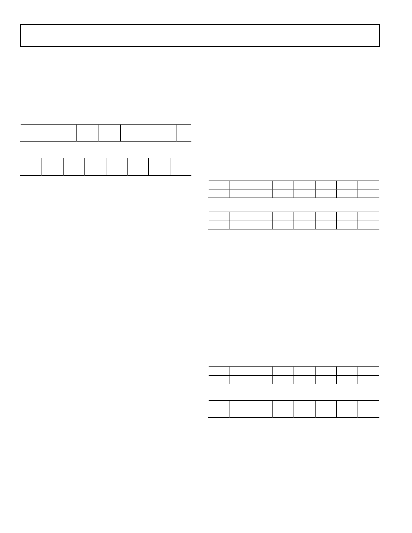
Table 13. Conversion Value Register (First Read)
D15
D14
D13
D12
Alert_Flag
CH
ID2
CH
ID1
CH
ID0
M S B B10
Table 14. Conversion Value Register (Second Read)
D7
D6
D5
D4
B7
B6
B5
B4
Rev. 0 | Page 20 of 32
D11
D10 D9
D8
B8
B9
D3
B3
D2
B2
D1
B1
D0
B0
The AD7997/AD7998 conversion result consists of an Alert_Flag
bit, three channel identifier bits, and the 10- and 12-bit data
result (MSB first). For the AD7997, the 2 LSBs (D1 and D0) of
the second read contain two 0s. The three channel identification
bits can be used to identify to which of the eight analog input
channels the conversion result corresponds.
The Alert_Flag bit indicates whether the conversion result being
read or any other channel result has violated the limit registers
associated with it. If an ALERT occurs, the master can read the
ALERT status register to obtain more information on where the
ALERT occurred.
LIMIT REGISTERS
The AD7997/AD7998 have four pairs of limit registers. Each
pair stores high and low conversion limits for the first four
analog input channels, CH1 to CH4. Each pair of limit registers
has one associated hysteresis register. All 12 registers are 16 bits
wide; only the 12 LSBs of the registers are used for the AD7997
and AD7998. For the AD7997, the 2 LSBs, D1 and D0 in these
registers, should contain 0s. On power-up, the contents of the
DATA
HIGH
register for each channel is full scale, while the
contents of the DATA
LOW
registers is zero scale by default. The
AD7997/AD7998 signal an alert (in either hardware, software,
or both depending on configuration) if the conversion result
moves outside the upper or lower limit set by the limit registers.
There are no limit registers or hysteresis registers associated
with CH5 to CH8.
DATA
HIGH
Register CH1/CH2/CH3/CH4
The DATA
HIGH
registers for CH1 to CH 4 are 16-bit read/write
registers; only the 12 LSBs of each register are used. This
register stores the upper limit that activates the ALERT output
and/or the Alert_Flag bit in the conversion result register. If the
value in the conversion result register is greater than the value
in the DATA
HIGH
register, an ALERT occurs for that channel.
When the conversion result returns to a value at least
N
LSBs
below the DATA
HIGH
register value, the ALERT output pin and
Alert_Flag bit are reset. The value of
N
is taken from the
hysteresis register associated with that channel. The ALERT pin
can also be reset by writing to Bits D2 and D1 in the
configuration register. For the AD7997, D1 and D0 of the
DATA
HIGH
register should contain 0s.
Table 15. DATA
HIGH
Register (First Read/Write)
D15
D14
D13
D12
0
0
0
0
Table 16. DATA
HIGH
Register (Second Read/Write)
D7
D6
D5
D4
B7
B6
B5
B4
D11
B11
D10
B10
D9
B9
D8
B8
D3
B3
D2
B2
D1
B1
D0
B0
DATA
LOW
Register CH1/CH2/CH3/CH4
The DATA
LOW
register for each channel is a 16-bit read/write
register; only the 12 LSBs of each register are used. The register
stores the lower limit that activates the ALERT output and/or
the Alert_Flag bit in the conversion result register. If the value
in the conversion result register is less than the value in the
DATA
LOW
register, an ALERT occurs for that channel. When the
conversion result returns to a value at least
N
LSBs above the
DATA
LOW
register value, the ALERT output pin and Alert_Flag
bit are reset. The value of
N
is taken from the hysteresis register
associated with that channel. The ALERT output pin can also be
reset by writing to Bits D2 and D1 in the configuration register.
For the AD7997, D1 to D0 of the DATA
LOW
register should
contain 0s.
Table 17. DATA
LOW
Register (First Read/Write)
D15
D14
D13
D12
0
0
0
0
Table 18. DATA
LOW
Register (Second Read/Write)
D7
D6
D5
D4
B7
B6
B5
B4
D11
B11
D10
B10
D9
B9
D8
B8
D3
B3
D2
B2
D1
B1
D0
B0
相關PDF資料 |
PDF描述 |
|---|---|
| AD7997BRUZ-0REEL3 | 8-Channel, 10- and 12-Bit ADCs with I2CCompatible |
| AD7997BRUZ-13 | 8-Channel, 10- and 12-Bit ADCs with I2CCompatible |
| AD7997BRUZ-1REEL3 | 8-Channel, 10- and 12-Bit ADCs with I2CCompatible |
| AD7998 | 8-Channel, 10- and 12-Bit ADCs with I2CCompatible |
| AD7998BRU-0 | 8-Channel, 10- and 12-Bit ADCs with I2CCompatible |
相關代理商/技術參數 |
參數描述 |
|---|---|
| AD7997BRUZ-0REEL | 功能描述:IC ADC 10BIT 8CHAN I2C 20TSSOP RoHS:是 類別:集成電路 (IC) >> 數據采集 - 模數轉換器 系列:- 標準包裝:2,500 系列:- 位數:16 采樣率(每秒):15 數據接口:MICROWIRE?,串行,SPI? 轉換器數目:1 功率耗散(最大):480µW 電壓電源:單電源 工作溫度:-40°C ~ 85°C 安裝類型:表面貼裝 封裝/外殼:38-WFQFN 裸露焊盤 供應商設備封裝:38-QFN(5x7) 包裝:帶卷 (TR) 輸入數目和類型:16 個單端,雙極;8 個差分,雙極 配用:DC1011A-C-ND - BOARD DELTA SIGMA ADC LTC2494 |
| AD7997BRUZ-0REEL3 | 制造商:AD 制造商全稱:Analog Devices 功能描述:8-Channel, 10- and 12-Bit ADCs with I2CCompatible |
| AD7997BRUZ-1 | 功能描述:IC ADC 10BIT 8CHAN I2C 20TSSOP RoHS:是 類別:集成電路 (IC) >> 數據采集 - 模數轉換器 系列:- 標準包裝:1 系列:microPOWER™ 位數:8 采樣率(每秒):1M 數據接口:串行,SPI? 轉換器數目:1 功率耗散(最大):- 電壓電源:模擬和數字 工作溫度:-40°C ~ 125°C 安裝類型:表面貼裝 封裝/外殼:24-VFQFN 裸露焊盤 供應商設備封裝:24-VQFN 裸露焊盤(4x4) 包裝:Digi-Reel® 輸入數目和類型:8 個單端,單極 產品目錄頁面:892 (CN2011-ZH PDF) 其它名稱:296-25851-6 |
| AD7997BRUZ-13 | 制造商:AD 制造商全稱:Analog Devices 功能描述:8-Channel, 10- and 12-Bit ADCs with I2CCompatible |
| AD7997BRUZ-1REEL | 功能描述:IC ADC 10BIT 8CHAN I2C 20TSSOP RoHS:是 類別:集成電路 (IC) >> 數據采集 - 模數轉換器 系列:- 標準包裝:2,500 系列:- 位數:16 采樣率(每秒):15 數據接口:MICROWIRE?,串行,SPI? 轉換器數目:1 功率耗散(最大):480µW 電壓電源:單電源 工作溫度:-40°C ~ 85°C 安裝類型:表面貼裝 封裝/外殼:38-WFQFN 裸露焊盤 供應商設備封裝:38-QFN(5x7) 包裝:帶卷 (TR) 輸入數目和類型:16 個單端,雙極;8 個差分,雙極 配用:DC1011A-C-ND - BOARD DELTA SIGMA ADC LTC2494 |
發布緊急采購,3分鐘左右您將得到回復。