- 您現在的位置:買賣IC網 > PDF目錄373927 > AD7998BRUZ-0REEL3 (Analog Devices, Inc.) 8-Channel, 10- and 12-Bit ADCs with I2CCompatible PDF資料下載
參數資料
| 型號: | AD7998BRUZ-0REEL3 |
| 廠商: | Analog Devices, Inc. |
| 元件分類: | 串行ADC |
| 英文描述: | 8-Channel, 10- and 12-Bit ADCs with I2CCompatible |
| 中文描述: | 8通道,10 -和12位ADC與I2CCompatible |
| 文件頁數: | 10/32頁 |
| 文件大小: | 1056K |
| 代理商: | AD7998BRUZ-0REEL3 |
第1頁第2頁第3頁第4頁第5頁第6頁第7頁第8頁第9頁當前第10頁第11頁第12頁第13頁第14頁第15頁第16頁第17頁第18頁第19頁第20頁第21頁第22頁第23頁第24頁第25頁第26頁第27頁第28頁第29頁第30頁第31頁第32頁
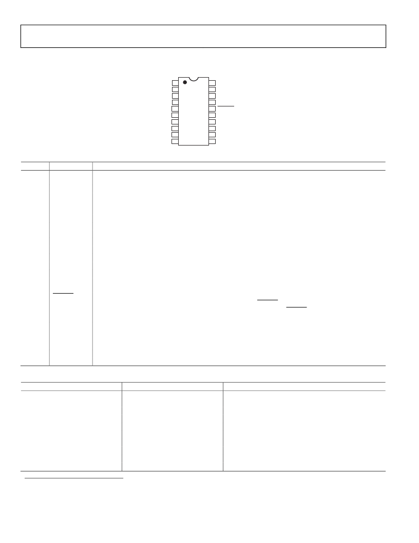
AD7997/AD7998
PIN CONFIGURATION AND PIN FUNCTION DESCRIPTIONS
Rev. 0 | Page 10 of 32
AD7997/
AD7998
TOP VIEW
5
(Not to Scale)
1
2
3
4
17
18
19
20
SDA
ALERT/BUSY
CONVST
SCL
V
DD
AGND
V
DD
AGND
AGND
V
IN
4
V
IN
6
14
13
V
IN
2
16
15
AS
AGND
REF
IN
V
IN
1
V
IN
3
V
IN
5
V
IN
7
6
7
8
9
10
V
IN
8
12
11
0
Figure 3. AD7998/AD7997 Pin Configuration
Table 5. Pin Function Descriptions
Pin No.
Mnemonic
1, 3,
4, 20
2, 5
V
DD
6
REF
IN
Function
Analog Ground. Ground reference point for all circuitry on the AD7997/AD7998. All analog input signals should be
referred to this AGND voltage.
Power Supply Input. The V
DD
range for the AD7997/AD7998 is from 2.7 V to 5.5 V.
Voltage Reference Input. The external reference for the AD7997/AD7998 should be applied to this input pin. The
voltage range for the external reference is 1.2 V to V
DD
. A 0.1 μF and 1 μF capacitors should be placed between REF
IN
and AGND. See Typical Connection Diagram.
Analog Input 1. Single-ended analog input channel. The input range is 0 V to REF
IN
.
Analog Input 3. Single-ended analog input channel. The input range is 0 V to REF
IN
.
Analog Input 5. Single-ended analog input channel. The input range is 0 V to REF
IN
.
Analog Input 7. Single-ended analog input channel. The input range is 0 V to REF
IN
.
Analog Input 8. Single-ended analog input channel. The input range is 0 V to REF
IN
.
Analog Input 6. Single-ended analog input channel. The input range is 0 V to REF
IN
.
Analog Input 4. Single-ended analog input channel. The input range is 0 V to REF
IN
.
Analog Input 2. Single-ended analog input channel. The input range is 0 V to REF
IN
.
Logic Input. Address select input that selects one of three I
2
C addresses for the AD7997/AD7998, as shown in Table
6
.
The device address depends on the voltage applied to this pin.
Logic Input Signal. Convert start signal. This is an edge-triggered logic input. The rising edge of this signal powers up
the part. The power-up time for the part is 1 μs. The falling edge of CONVST places the track/hold into hold mode and
initiates a conversion. A power-up time of at least 1 μs must be allowed for the CONVST high pulse; otherwise, the
conversion result is invalid (see the Modes of Operation section).
Digital Output. Selectable as an ALERT or BUSY output function. When configured as an ALERT, this pin acts as an out-
of-range indicator and, if enabled, becomes active when the conversion result violates the DATAHIGH or DATALOW
register values. See the Limit Registers section. When configured as a BUSY output, this pin becomes active when a
conversion is in progress. Open-drain output.
Digital I/O. Serial bus bidirectional data. Open-drain output. External pull-up resistor required.
Digital Input. Serial bus clock. Open-drain input. External pull-up resistor required.
AGND
7
8
9
10
11
12
13
14
15
V
IN
1
V
IN
3
V
IN
5
V
IN
7
V
IN
8
V
IN
6
V
IN
4
V
IN
2
AS
16
CONVST
17
ALERT/BUSY
18
19
Table 6. I
2
C Address Selection
Part Number
AD7997-0
AD7997-0
AD7997-1
AD7997-1
AD7997-x
1
AD7998-0
AD7998-0
AD7998-1
AD7998-1
AD7998-x
1
SDA
SCL
AS Pin
AGND
V
DD
AGND
V
DD
Float
AGND
V
DD
AGND
V
DD
Float
I
2
C Address
010 0001
010 0010
010 0011
010 0100
010 0000
010 0001
010 0010
010 0011
010 0100
010 0000
1
If the AS pin is left floating on any of the AD7997/AD7998 parts, the device address is 010 0000.
相關PDF資料 |
PDF描述 |
|---|---|
| AD7998BRUZ-13 | 8-Channel, 10- and 12-Bit ADCs with I2CCompatible |
| AD7998BRUZ-1REEL3 | 8-Channel, 10- and 12-Bit ADCs with I2CCompatible |
| AD8005AR-REEL7 | 270 MHz, 400 uA Current Feedback Amplifier |
| AD8005ART-REEL | 270 MHz, 400 uA Current Feedback Amplifier |
| AD8005ART-REEL7 | 270 MHz, 400 uA Current Feedback Amplifier |
相關代理商/技術參數 |
參數描述 |
|---|---|
| AD7998BRUZ-1 | 功能描述:IC ADC 12BIT 8CH W/I2C 20-TSSOP RoHS:是 類別:集成電路 (IC) >> 數據采集 - 模數轉換器 系列:- 標準包裝:1 系列:microPOWER™ 位數:8 采樣率(每秒):1M 數據接口:串行,SPI? 轉換器數目:1 功率耗散(最大):- 電壓電源:模擬和數字 工作溫度:-40°C ~ 125°C 安裝類型:表面貼裝 封裝/外殼:24-VFQFN 裸露焊盤 供應商設備封裝:24-VQFN 裸露焊盤(4x4) 包裝:Digi-Reel® 輸入數目和類型:8 個單端,單極 產品目錄頁面:892 (CN2011-ZH PDF) 其它名稱:296-25851-6 |
| AD7998BRUZ-13 | 制造商:AD 制造商全稱:Analog Devices 功能描述:8-Channel, 10- and 12-Bit ADCs with I2CCompatible |
| AD7998BRUZ-1REEL | 功能描述:IC ADC 12BIT 8CHAN I2C 20TSSOP RoHS:是 類別:集成電路 (IC) >> 數據采集 - 模數轉換器 系列:- 標準包裝:1,000 系列:- 位數:16 采樣率(每秒):45k 數據接口:串行 轉換器數目:2 功率耗散(最大):315mW 電壓電源:模擬和數字 工作溫度:0°C ~ 70°C 安裝類型:表面貼裝 封裝/外殼:28-SOIC(0.295",7.50mm 寬) 供應商設備封裝:28-SOIC W 包裝:帶卷 (TR) 輸入數目和類型:2 個單端,單極 |
| AD7998BRUZ-1REEL3 | 制造商:AD 制造商全稱:Analog Devices 功能描述:8-Channel, 10- and 12-Bit ADCs with I2CCompatible |
| AD7999 | 制造商:AD 制造商全稱:Analog Devices 功能描述:4-Channel, 12-/10-/8-Bit ADC with I2C-Compatible Interface in 8-Lead SOT-23 |
發布緊急采購,3分鐘左右您將得到回復。