- 您現(xiàn)在的位置:買賣IC網(wǎng) > PDF目錄373928 > AD8005AN (ANALOG DEVICES INC) 270 MHz, 400 uA Current Feedback Amplifier PDF資料下載
參數(shù)資料
| 型號: | AD8005AN |
| 廠商: | ANALOG DEVICES INC |
| 元件分類: | 運(yùn)動控制電子 |
| 英文描述: | 270 MHz, 400 uA Current Feedback Amplifier |
| 中文描述: | OP-AMP, 50000 uV OFFSET-MAX, PDIP8 |
| 封裝: | PLASTIC, DIP-8 |
| 文件頁數(shù): | 10/12頁 |
| 文件大小: | 183K |
| 代理商: | AD8005AN |
AD8005
–10–
REV. A
Single-Ended-to-Differential Conversion
Many single supply ADCs have differential inputs. In such cases,
the ideal common-mode operating point is usually halfway
between supply and ground. Figure 31 shows how to convert a
single-ended bipolar signal into a differential signal with a
common-mode level of 2.5 V.
0.1
m
F
0.1
m
F
+5V
R
IN
1k
V
AD8005
2.49k
V
0.1
m
F
BIPOLAR
SIGNAL
6
0.5V
+5V
2.49k
V
2.49k
V
+5V
AD8005
0.1
m
F
2.49k
V
+5V
V
OUT
R
F1
2.49k
V
R
F2
3.09k
V
R
G
619
V
Figure 31. Single-Ended-to-Differential Converter
Amp 1 has its +input driven with the ac-coupled input signal
while the +input of Amp 2 is connected to a bias level of +2.5 V.
Thus the –input of Amp 2 is driven to virtual +2.5 V by its
output. Therefore, Amp 1 is configured for a noninverting gain
of five, (1 + R
F1
/R
G
), because RG is connected to the virtual
+2.5 V of Amp 2’s –input.
When the +input of Amp 1 is driven with a signal, the same
signal appears at the –input of Amp 1. This signal serves as an
input to Amp 2 configured for a gain of –5, (–R
F2
/R
G
). Thus the
two outputs move in opposite directions with the same gain and
create a balanced differential signal.
This circuit can be simplified to create a bipolar in/bipolar out
single-ended to differential converter. Obviously, a single supply
is no longer adequate and the –V
S
pins must now be powered
with –5 V. The +input to Amp 2 is tied to ground. The ac
coupling on the +input of Amp 1 is removed and the signal can
be fed directly into Amp 1.
Layout Considerations
In order to achieve the specified high-speed performance of the
AD8005 you must be attentive to board layout and component
selection. Proper R
F
design techniques and selection of compo-
nents with low parasitics are necessary.
The PCB should have a ground plane that covers all unused
portions of the component side of the board. This will provide a
low impedance path for signals flowing to ground. The ground
plane should be removed from the area under and around the
chip (leave about 2 mm between the pin contacts and the
ground plane). This helps to reduce stray capacitance. If both
signal tracks and the ground plane are on the same side of the
PCB, also leave a 2 mm gap between ground plane and track.
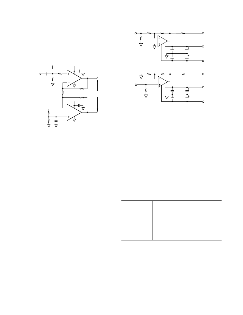
C1
0.01
m
F
C2
0.01
m
F
C4
10
m
F
C3
10
m
F
R
T
INVERTING CONFIGURATION
V
IN
V
OUT
+V
S
–V
S
R
G
R
F
R
O
C1
0.01
m
F
C2
0.01
m
F
C4
10
m
F
C3
10
m
F
R
T
NONINVERTING CONFIGURATION
V
IN
V
OUT
+V
S
–V
S
R
G
R
F
R
O
Figure 32. Inverting and Noninverting Configurations
Chip capacitors have low parasitic resistance and inductance
and are suitable for supply bypassing (see Figure 32). Make sure
that one end of the capacitor is within 1/8 inch of each power
pin with the other end connected to the ground plane. An
additional large (0.47
μ
F–10
μ
F) tantalum electrolytic capacitor
should also be connected in parallel. This capacitor supplies
current for fast, large signal changes at the output. It must not
necessarily be as close to the power pin as the smaller capacitor.
Locate the feedback resistor close to the inverting input pin in
order to keep the stray capacitance at this node to a minimum.
Capacitance variations of less than 1.5 pF at the inverting input
will significantly affect high-speed performance.
Use stripline design techniques for long signal traces (i.e., greater
than about 1 inch). Striplines should have a characteristic
impedance of either 50
or 75
. For the Stripline to be
effective, correct termination at both ends of the line is necessary.
Table I. Typical Bandwidth vs. Gain Setting Resistors
Small Signal –3 dB
BW (MHz),
V
S
=
6
5 V
Gain
R
F
R
G
R
T
–1
–10
+1
+2
+10
1.49 k
1 k
2.49 k
2.49 k
499
1.49 k
100
`
2.49 k
56.2
52.3
100
49.9
49.9
49.9
120 MHz
60 MHz
270 MHz
170 MHz
40 MHz
相關(guān)PDF資料 |
PDF描述 |
|---|---|
| AD8005AR | 270 MHz, 400 uA Current Feedback Amplifier |
| AD8005AR-REEL | 270 MHz, 400 uA Current Feedback Amplifier |
| AD8009 | 1 GHz, 5,500 V/us Low Distortion Amplifier |
| AD8009AR | 1 GHz, 5,500 V/us Low Distortion Amplifier |
| AD8009ART | 1 GHz, 5,500 V/us Low Distortion Amplifier |
相關(guān)代理商/技術(shù)參數(shù) |
參數(shù)描述 |
|---|---|
| AD8005ANZ | 功能描述:IC OPAMP CF ULP LDIST 10MA 8DIP RoHS:是 類別:集成電路 (IC) >> Linear - Amplifiers - Instrumentation 系列:- 產(chǎn)品培訓(xùn)模塊:Differential Circuit Design Techniques for Communication Applications 標(biāo)準(zhǔn)包裝:1 系列:- 放大器類型:RF/IF 差分 電路數(shù):1 輸出類型:差分 轉(zhuǎn)換速率:9800 V/µs 增益帶寬積:- -3db帶寬:2.9GHz 電流 - 輸入偏壓:3µA 電壓 - 輸入偏移:- 電流 - 電源:40mA 電流 - 輸出 / 通道:- 電壓 - 電源,單路/雙路(±):3 V ~ 3.6 V 工作溫度:-40°C ~ 85°C 安裝類型:表面貼裝 封裝/外殼:16-VQFN 裸露焊盤,CSP 供應(yīng)商設(shè)備封裝:16-LFCSP-VQ 包裝:剪切帶 (CT) 產(chǎn)品目錄頁面:551 (CN2011-ZH PDF) 其它名稱:ADL5561ACPZ-R7CT |
| AD8005AR | 制造商:Analog Devices 功能描述:OP Amp Single Current Fdbk 制造商:Rochester Electronics LLC 功能描述:SOIC 180MHZ,400UA CURRENT FEEDBACK AMP - Bulk 制造商:Analog Devices 功能描述:IC AMP ULTRA LOW POWER |
| AD8005AR-EBZ | 功能描述:BOARD EVAL FOR AD8005AR RoHS:是 類別:編程器,開發(fā)系統(tǒng) >> 評估板 - 運(yùn)算放大器 系列:- 產(chǎn)品培訓(xùn)模塊:Lead (SnPb) Finish for COTS Obsolescence Mitigation Program 標(biāo)準(zhǔn)包裝:1 系列:- |
| AD8005AR-REEL | 制造商:Analog Devices 功能描述:OP Amp Single Current Fdbk 制造商:Rochester Electronics LLC 功能描述:SOIC 180MHZ,400UA CURRENT FEEDBACK AMP - Tape and Reel |
| AD8005AR-REEL7 | 制造商:Analog Devices 功能描述:OP Amp Single Current Fdbk 制造商:Rochester Electronics LLC 功能描述:SOIC 180MHZ,400UA CURRENT FEEDBACK AMP - Tape and Reel |
發(fā)布緊急采購,3分鐘左右您將得到回復(fù)。