- 您現在的位置:買賣IC網 > PDF目錄373929 > AD8016ARB-REEL (ANALOG DEVICES INC) Circular Connector; No. of Contacts:5; Series:; Body Material:Aluminum Alloy; Connecting Termination:Solder; Connector Shell Size:22; Circular Contact Gender:Socket; Circular Shell Style:Wall Mount Receptacle RoHS Compliant: No PDF資料下載
參數資料
| 型號: | AD8016ARB-REEL |
| 廠商: | ANALOG DEVICES INC |
| 元件分類: | 運動控制電子 |
| 英文描述: | Circular Connector; No. of Contacts:5; Series:; Body Material:Aluminum Alloy; Connecting Termination:Solder; Connector Shell Size:22; Circular Contact Gender:Socket; Circular Shell Style:Wall Mount Receptacle RoHS Compliant: No |
| 中文描述: | DUAL OP-AMP, 3000 uV OFFSET-MAX, PDSO24 |
| 封裝: | BATWING, SOIC-24 |
| 文件頁數: | 14/20頁 |
| 文件大小: | 569K |
| 代理商: | AD8016ARB-REEL |
REV. A
AD8016
–14–
we can use symmetry to simplify the computation for a dc input
signal.
P
I
V
V
(
V
V
R
D
Q
S
S
O
O
L
=
×
×
+
×
2
4
–
)
where
V
O
is the peak output voltage of an amplifier.
This formula is slightly pessimistic due to the fact that some of
the quiescent supply current is commutated during sourcing or
sinking current into the load. For a sine wave source, integration
over a half cycle yields:
P
I
V
V V
R
π
V
R
D
Q
S
S
L
O
L
=
×
×
+
2
2
4
2
The situation is more complicated with a complex modulated
signal. In the case of a DMT signal, taking the equivalent sine
wave power overestimates the power dissipation by ~23%. For
example:
P
OUT
= 23.4
dBm
= 220
mW
V
OUT
@ 50
= 3.31
V rms
V
O
= 2.354
V
at each amplifier output, which yields a P
D
of 1.81 W.
Through measurement, a DMT signal of 23.4 dBm requires
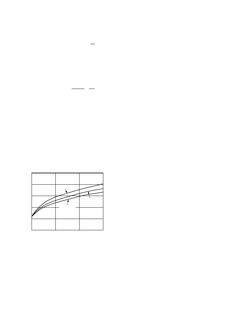
1.47 W of power to be dissipated by the AD8016. Figure 41
shows the results of calculation and actual measurements
detailing the relationship between the power dissipated by the
AD8016 versus the total output power delivered to the back
termination resistors and the load combined. A 1:2 transformer
turns ratio was used in the calculations and measurements.
OUTPUT POWER
–
mW
2.5
0
P
2.0
1.5
100
200
300
1.0
0.5
0
MEASURED
SINE
MEASURED
DMT
CALCULATED
Figure 41. Power Dissipation vs. Output Power (Including
Back Terminations). See Figure 7 for Test Circuit
THERMAL ENHANCEMENTS AND PCB LAYOUT
There are several ways to enhance the thermal capacity of the
CO solution. Additional thermal capacity can be created using
enhanced PCB layout techniques such as interlacing (sometimes
referred to as stitching or interconnection) of the layers immedi-
ately beneath the line driver. This technique serves to increase
the thermal mass or capacity of the PCB immediately beneath
the driver. (See AD8016-EVAL boards for an example of this
method of thermal enhancement.) A cooling fan that draws
moving air over the PCB and xDSL drivers, while not always
required, may be useful in reducing the operating temperature
of the die, allowing more drivers/square-inch within the CO
design. The AD8016, whether in a PSOP3 (ARP) or batwing
(ARB) package, can be designed to operate in the CO solution
using prudent measures to manage the power dissipation through
careful PCB design. The PSOP3 package is available for use in
designing the highest density CO solutions. Maximum heat trans-
fer to the PCB can be accomplished using the PSOP3 package
when the thermal slug is soldered to an exposed copper pad
directly beneath the AD8016. Optimum thermal performance
can be achieved in the ARE package only when the back of the
package is soldered to a PCB designed for maximum thermal
capacity (see Figure 44). Thermal experiments with the PS0P3
package were conducted
without
soldering the heat slug to the
PCB. Heat transfer was through physical contact only. The
following offers some insight into the AD8016 power dissipation
and relative junction temperature, the effects of PCB size and
composition on the junction-to-air thermal resistance or
θ
JA
.
THERMAL TESTING
A wind tunnel study was conducted to determine the relationship
between thermal capacity (i.e., printed circuit board copper area),
air flow and junction temperature. Junction-to-ambient ther-
mal resistance,
θ
JA
, was also calculated for the AD8016ARP,
AD8016ARE, and AD8016ARB packages. The AD8016 was
operated in a noninverting differential driver configuration, typical
of an xDSL application yet isolated from any other modem
components. Testing was conducted using a 1 ounce copper
board in an ambient temperature of ~24
°
C over air flows of
200, 150, 100, and 50 (0.200 and 400 for AD8016ARE) linear
feet per minute (LFM) and for ARP and ARB packages as well
as in still air. The four-layer PCB was designed to maximize the
area of copper on the outer two layers of the board while the
inner layers were used to configure the AD8016 in a differential
driver circuit. The PCB measured 3
×
4 inches in the beginning
of the study and was progressively reduced in size to approxi-
mately 2
×
2 inches. The testing was performed in a wind tunnel to
control air flow in units of LFM. The tunnel is approximately
11 inches in diameter.
AIR FLOW TEST CONDITIONS
DUT Power:
Typical DSL DMT signal produces about 1.5 W
of power dissipation in the AD8016 package. The fully biased
(PWDN0 and PWDN1 = Logic 1) quiescent current of the
AD8016 is ~25 mA. A 1 MHz differential sine wave at an ampli-
tude of 8 V p-p/amplifier into an R
LOAD
of 100
differential
(50
per side) will produce the 1.5 W of power typical in the
AD8016 device. (See the Power Dissipation section for details.)
Thermal Resistance:
The junction-to-case thermal resistance
(
θ
JC
) of the AD8016ARB or batwing package is 8.6
°
C/W,
AD8016ARE is 5.6
°
C/W, and the AD8016ARP or PSOP3
package is 0.86
°
C/W. These package specifications were used in
this study to determine junction temperature based on the mea-
sured case temperature.
PCB Dimensions of a Differential Driver Circuit:
Several
components are required to support the AD8016 in a differential
driver circuit. The PCB area necessary for these components (i.e.,
feedback and gain resistors, ac coupling and decoupling capaci-
tors, termination and load resistors) dictated the area of the
smallest PCB in this study, 4.7 square inches. Further reduction
in PCB area, although possible, will have consequences in terms
of the maximum operating junction temperature.
相關PDF資料 |
PDF描述 |
|---|---|
| AD8016ARE-EVAL | Low Power, High Output Current xDSL Line Driver |
| AD8016ARE-REEL | Low Power, High Output Current xDSL Line Driver |
| AD8016ARP-EVAL | Low Power, High Output Current xDSL Line Driver |
| AD8016ARP-REEL | Low Power, High Output Current xDSL Line Driver |
| AD8016 | Low Power, High Output Current xDSL Line Driver |
相關代理商/技術參數 |
參數描述 |
|---|---|
| AD8016ARBZ | 功能描述:IC AMP XDSL LINE DVR 24-SOIC RoHS:是 類別:集成電路 (IC) >> 接口 - 驅動器,接收器,收發器 系列:- 產品培訓模塊:RS-232 & USB Transceiver 標準包裝:2,000 系列:- 類型:收發器 驅動器/接收器數:1/1 規程:RS232 電源電壓:3 V ~ 5.5 V 安裝類型:表面貼裝 封裝/外殼:16-SSOP(0.209",5.30mm 寬) 供應商設備封裝:16-SSOP 包裝:帶卷 (TR) 其它名稱:296-19849-2 |
| AD8016ARBZ | 制造商:Analog Devices 功能描述:LINE DRIVER, DUAL, 1000 V/us, WSOIC-24 |
| AD8016ARBZ-REEL | 功能描述:IC AMP XDSL LINE DVR 24-SOIC TR RoHS:是 類別:集成電路 (IC) >> 接口 - 驅動器,接收器,收發器 系列:- 標準包裝:27 系列:- 類型:收發器 驅動器/接收器數:3/3 規程:RS232,RS485 電源電壓:4.75 V ~ 5.25 V 安裝類型:表面貼裝 封裝/外殼:28-SOIC(0.295",7.50mm 寬) 供應商設備封裝:28-SOIC 包裝:管件 |
| AD8016ARE | 制造商:Analog Devices 功能描述:ADSL Driver Dual 28-Pin TSSOP EP Tube 制造商:Rochester Electronics LLC 功能描述:TSSOP LOW POWER, HIGH OUTPUT CURRENT AMP - Bulk |
| AD8016ARE-EVAL | 功能描述:BOARD EVAL FOR AD8016ARE RoHS:否 類別:編程器,開發系統 >> 評估演示板和套件 系列:- 標準包裝:1 系列:- 主要目的:電信,線路接口單元(LIU) 嵌入式:- 已用 IC / 零件:IDT82V2081 主要屬性:T1/J1/E1 LIU 次要屬性:- 已供物品:板,電源,線纜,CD 其它名稱:82EBV2081 |
發布緊急采購,3分鐘左右您將得到回復。