- 您現(xiàn)在的位置:買賣IC網(wǎng) > PDF目錄373929 > AD8017 (Analog Devices, Inc.) Dual High Output Current, High Speed Amplifier PDF資料下載
參數(shù)資料
| 型號: | AD8017 |
| 廠商: | Analog Devices, Inc. |
| 元件分類: | 運動控制電子 |
| 英文描述: | Dual High Output Current, High Speed Amplifier |
| 中文描述: | 雙路高輸出電流,高速放大器 |
| 文件頁數(shù): | 14/16頁 |
| 文件大小: | 223K |
| 代理商: | AD8017 |
AD8017
–14–
REV. A
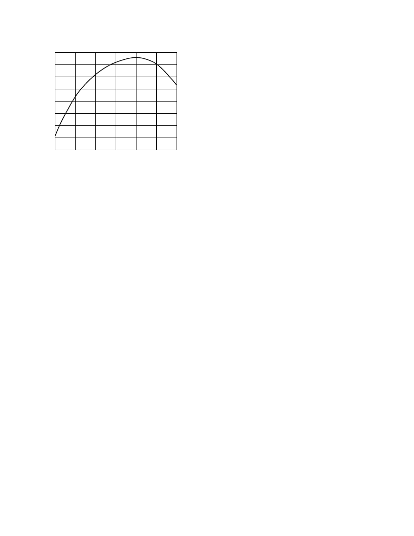
OUTPUT VOLTAGE (V
O
)
–
V
PK
P
D
)
–
0.8
0
0.2
4
1
2
0
3
0.3
0.4
0.5
0.6
0.7
0.1
5
6
Figure 41. Power Dissipation (P
D
) vs. Output Voltage (V
O
),
R
L
= 50
Thermal Considerations
The AD8017 in a
“
Thermal Coastline
”
SO-8 package relies on
the device pins to assist in removing heat from the die at a faster
rate than that of conventional packages. The effect is to provide
a lower
θ
JC
for the device. To make the most effective use of
this, special details should be worked into the copper traces of
the printed circuit board.
There will be a tradeoff, however, between designing a board
that will maximally remove heat, and one that will provide the
desired ac performance. This is the result of the additional para-
sitic capacitance on some of the pins that would be caused by
the addition of extra heatsinking copper traces.
The first technique for maximum heatsinking is to use a heavy
layer of copper. 2 oz. copper will provide better heatsinking than
1 oz. copper. Additional internal circuit layers can also be used
to more effectively remove heat, and to provide better power
and ground distribution.
There are no
“
ground
”
pins per se on the AD8017 (when run
on a dual supply), but the power supplies (Pins 4 and 8) are at
ac ground. Thus, these pins can be safely tied to a maximum
area of copper foil without affecting the ac performance of the
part. On the surface side of the board, the copper area that
connects to Pins 4 and 8 should be enlarged and spread out to
the maximum extent possible. As a practical matter, there will
be diminishing returns from adding copper more than a few
centimeters from the pins.
When the power supplies are run on the board on internal
power planes, then these should also be made as large as practi-
cal, and multiple vias (~0.012 in. or 0.3 mm) should be pro-
vided from the component layer near the power supply pins of
the AD8017 to the inner layers. These vias should not have any
of the traditional
“
thermal relief
”
spokes to the planes, because
the function of these is to impede heat flow for ease of soldering.
This is counter to the effect desired for heatsinking.
On the side of the board opposite the component, additional
heatsinking can be provided by adding copper area near the vias
to further lower the thermal resistance. Additional vias can be
provided throughout to better conduct heat from the inner
layers to the outer layers.
The remainder of the device pins are active signal pins and must
be treated a bit more carefully. Pins 2 and 6 are the summing
junctions of the op amps and will be the most adversely affected by
stray capacitance. For this reason, the copper area of these pins
should be minimized. In addition, the copper nearby on the
component layer should be kept more than 3 mm
–
5 mm away
from these pins, where possible. The inner and opposite side
circuit layers directly below the summing junctions should also
be void of copper.
The positive inputs and outputs can withstand somewhat more
capacitance than the summing junctions without adversely af-
fecting ac performance. However, these pins should be treated
carefully, and the amount of heatsinking and excess capacitance
should be analyzed and adjusted depending on the application.
If maximum ac performance is desired and the power dissipa-
tion is not extreme, then the copper area connected to these
pins should be minimized. If the ac performance is not very
critical and maximum power must be dissipated, then the cop-
per area connected to these pins can be increased. As in many
other areas of analog design, the designer must use some judg-
ment based on the consideration of the above, in order to pro-
duce a satisfactory design.
相關(guān)PDF資料 |
PDF描述 |
|---|---|
| AD8017AR | Dual High Output Current, High Speed Amplifier |
| AD8017AR-EVAL | Dual High Output Current, High Speed Amplifier |
| AD8017AR-REEL | Dual High Output Current, High Speed Amplifier |
| AD8017AR-REEL7 | Dual High Output Current, High Speed Amplifier |
| AD8018ARU-EVAL | 5 V, Rail-to-Rail, High-Output Current, xDSL Line Drive Amplifier |
相關(guān)代理商/技術(shù)參數(shù) |
參數(shù)描述 |
|---|---|
| AD8017_02 | 制造商:AD 制造商全稱:Analog Devices 功能描述:Dual High Output Current, High Speed Amplifier |
| AD80172 | 制造商:Analog Devices 功能描述: |
| AD80175-1 | 制造商:Analog Devices 功能描述: |
| AD80175-2 | 制造商:Analog Devices 功能描述: |
| AD80176YSVZ | 制造商:Analog Devices 功能描述:- Rail/Tube |
發(fā)布緊急采購,3分鐘左右您將得到回復。