- 您現(xiàn)在的位置:買賣IC網(wǎng) > PDF目錄373929 > AD8017AR-REEL7 (ANALOG DEVICES INC) Dual High Output Current, High Speed Amplifier PDF資料下載
參數(shù)資料
| 型號: | AD8017AR-REEL7 |
| 廠商: | ANALOG DEVICES INC |
| 元件分類: | 運動控制電子 |
| 英文描述: | Dual High Output Current, High Speed Amplifier |
| 中文描述: | DUAL OP-AMP, 2600 uV OFFSET-MAX, 100 MHz BAND WIDTH, PDSO8 |
| 封裝: | SOIC-8 |
| 文件頁數(shù): | 12/16頁 |
| 文件大小: | 223K |
| 代理商: | AD8017AR-REEL7 |
AD8017
–12–
REV. A
APPLICATIONS
Output Power Characteristics as Applied to ADSL Signals
The AD8017 was designed to provide both relatively high cur-
rent and voltage output capability. Figures 17 and 20 quantify
the ac load current versus distortion of the device at loads of
100
and 25
at 1 MHz. Using approximately –50 dBc as the
worst case distortion limit, the AD8017 exhibits acceptable
linearity to within approximately 1.4 V of either supply rail (12 V
or
±
6 V) while simultaneously providing 200 mA of load cur-
rent. These levels are achieved at only 7 mA of quiescent cur-
rent for each amplifier.
ADSL applications require signal line powers of 13 dBm that
can randomly peak to an instantaneous power (or V
×
I product)
of 28.5 dBm. This equates to peak-to-rms voltage ratio of 5.3-
to-1. Using a 1:2 transformer in the ADSL circuit illustrated
below and 100
as the line resistance, a peak voltage of 4.2 V
at a peak current of 168 mA will be required from the line driver
output (see Table I). See detailed application below. A higher
turns ratio transformer can be used to reduce the primary out-
put voltage swing of the amplifier (for devices that do not have
the voltage swing, but do have the current drive capability).
However, this requires more than an equivalent increase in
current due to the added I
×
R losses from the transformer for
the same receiver power. Generally this will result in added
distortion. Table I below shows the ADSL ac current and volt-
ages required for both a 1:1 and 1:2 transformer turns ratio.
V
IN
1k
1k
0.1 F
0.1 F
8
2
3
1
7
5
6
4.7V
4.7V
V
OUT
1:2
+12V
1k
0.1 F
169
169
4
1k
1 F
1 F
0.1 F
10 F
12.5
12.5
100
AD8017
50
EFFECTIVE
LOAD
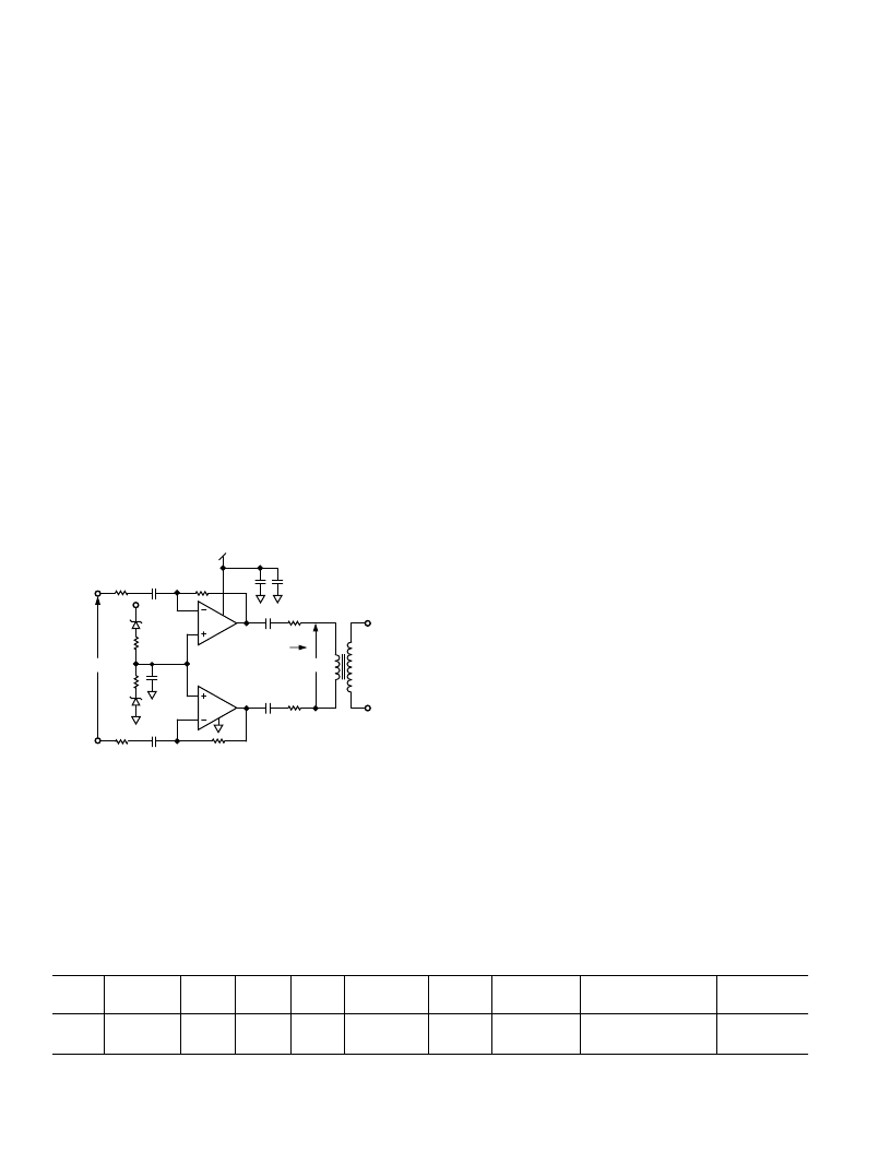
Figure 39. Single +12 V Supply ADSL Remote Terminal
Transmitter
Table I. DSL Drive Amplifier Requirements for Various Combinations of Line Power, Line Impedance and Turn Ratios
Line
Power
Insertion
Loss
Line
Load
100
100
Turns
Ratio
Crest
Factor
Reflected
Impedance
100
25
Per Amp
Voltage
Peak Per Amplifier
Voltage Output
Peak Current
Output
R1 = R2
50
12.5
13 dBm
13 dBm
1 dB
1 dB
1:1
1:2
5.3
5.3
1.585 V rms
0.792 V rms
8.4 V peak
4.2 V peak
84 mA
168 mA
Single +12 V Supply ADSL Remote Terminal (RT) Transmitter
For consumer use, it is desirable to create an ADSL modem
that can be a plug-in accessory for a PC. In such an application,
the circuit should dissipate a minimum of power, yet still meet
the ADSL specification.
The circuit in Figure 39 shows a single +12 V supply circuit
that uses the AD8017 as a remote terminal transmitter. This
supply voltage is readily available on the PCI connector of PCs.
The circuit configures each half of the AD8017 as an inverter
with a gain of about six. Both of the amplifier circuits are ac
coupled at both the inputs and the outputs. This makes the dc
levels of the circuit independent of the other dc levels of the
signal chain.
The inputs will generally be driven by the output of an active
filter, which has a low output impedance. Thus there will be a
minimum of loading of the source caused by the 169
input
impedance in the pass band. The output will require a 1:2 step-
up transformer to drive a 100
line. The reflected impedance
back to the primary will be 25
. With 25
of series termina-
tion added (12.5
in each output), the effective load that the
differential amplifier outputs will drive is 50
.
The input and output ac coupling provides two high pass cir-
cuits. The inputs are formed by the 0.1
μ
F capacitor and the
169
resistor, which provides a break frequency of about
9.4 kHz. The two 1
μ
F capacitors in the output along with the
50
effective load provides a 6.4 kHz break frequency in the
output side. Both of these circuits want to reject the Plain Old
Telephone System (POTS) band (dc to 4 kHz) while passing
the ADSL upstream band, which starts at about 20 kHz.
The positive inputs must be biased at mid supply, which is
nominally +6 V. This will maintain the maximum dynamic
range of the output in each direction, regardless of the tolerance
of the supply. The inverting configuration was chosen as this
requires a steady dc current from this supply, as opposed to the
signal-dependent current that would be required in a noninvert-
ing configuration. Several options were studied for creating this
supply.
A voltage regulator could be used, but there are several disad-
vantages. The first is that this will not track the middle of the
supplies as it will always have an output that is a fixed voltage
from ground. This also requires an additional active component
that will impact the cost of the total solution.
A two-resistor divider could also be used. There is a tradeoff
required here in the selection of the value of the resistors. As the
resistors become smaller, the amount of power that they will
dissipate will increase. For two 1 k
resistors, the power dissi-
pation in this circuit would be 72 mW. Thus, in order to keep
this power to a minimum, it is desirable to make the resistors as
large as possible.
相關(guān)PDF資料 |
PDF描述 |
|---|---|
| AD8018ARU-EVAL | 5 V, Rail-to-Rail, High-Output Current, xDSL Line Drive Amplifier |
| AD8018ARU-REEL | 5 V, Rail-to-Rail, High-Output Current, xDSL Line Drive Amplifier |
| AD8018 | RESISTOR-FIXED, METAL |
| AD8018AR | 5 V, Rail-to-Rail, High-Output Current, xDSL Line Drive Amplifier |
| AD8018ARU | 5 V, Rail-to-Rail, High-Output Current, xDSL Line Drive Amplifier |
相關(guān)代理商/技術(shù)參數(shù) |
參數(shù)描述 |
|---|---|
| AD8017ARZ | 功能描述:IC AMP GP DUAL LP LDIST 8SOIC RoHS:是 類別:集成電路 (IC) >> Linear - Amplifiers - Instrumentation 系列:- 標(biāo)準(zhǔn)包裝:2,500 系列:- 放大器類型:通用 電路數(shù):4 輸出類型:- 轉(zhuǎn)換速率:0.6 V/µs 增益帶寬積:1MHz -3db帶寬:- 電流 - 輸入偏壓:45nA 電壓 - 輸入偏移:2000µV 電流 - 電源:1.4mA 電流 - 輸出 / 通道:40mA 電壓 - 電源,單路/雙路(±):3 V ~ 32 V,±1.5 V ~ 16 V 工作溫度:0°C ~ 70°C 安裝類型:表面貼裝 封裝/外殼:14-TSSOP(0.173",4.40mm 寬) 供應(yīng)商設(shè)備封裝:14-TSSOP 包裝:帶卷 (TR) 其它名稱:LM324ADTBR2G-NDLM324ADTBR2GOSTR |
| AD8017ARZ-REEL | 功能描述:IC AMP GP DUAL LP LDIST 8SOIC RoHS:是 類別:集成電路 (IC) >> Linear - Amplifiers - Instrumentation 系列:- 其它有關(guān)文件:Automotive Product Guide 產(chǎn)品培訓(xùn)模塊:Lead (SnPb) Finish for COTS Obsolescence Mitigation Program 標(biāo)準(zhǔn)包裝:1 系列:- 放大器類型:通用 電路數(shù):1 輸出類型:滿擺幅 轉(zhuǎn)換速率:3 V/µs 增益帶寬積:10MHz -3db帶寬:- 電流 - 輸入偏壓:1pA 電壓 - 輸入偏移:70µV 電流 - 電源:2.5mA 電流 - 輸出 / 通道:48mA 電壓 - 電源,單路/雙路(±):2.7 V ~ 5.5 V,±1.35 V ~ 2.75 V 工作溫度:-40°C ~ 125°C 安裝類型:表面貼裝 封裝/外殼:SOT-23-6 供應(yīng)商設(shè)備封裝:SOT-6 包裝:Digi-Reel® 其它名稱:MAX4475AUT#TG16DKR |
| AD8017ARZ-REEL7 | 功能描述:IC AMP GP DUAL LP LDIST 8SOIC RoHS:是 類別:集成電路 (IC) >> Linear - Amplifiers - Instrumentation 系列:- 產(chǎn)品培訓(xùn)模塊:Lead (SnPb) Finish for COTS Obsolescence Mitigation Program 標(biāo)準(zhǔn)包裝:1 系列:- 放大器類型:電流檢測 電路數(shù):1 輸出類型:- 轉(zhuǎn)換速率:- 增益帶寬積:125kHz -3db帶寬:- 電流 - 輸入偏壓:- 電壓 - 輸入偏移:100µV 電流 - 電源:1.1µA 電流 - 輸出 / 通道:- 電壓 - 電源,單路/雙路(±):- 工作溫度:-40°C ~ 85°C 安裝類型:表面貼裝 封裝/外殼:4-WFBGA,CSPBGA 供應(yīng)商設(shè)備封裝:4-UCSP(2x2) 包裝:剪切帶 (CT) 其它名稱:MAX9634WERS+TCT |
| AD8018 | 制造商:AD 制造商全稱:Analog Devices 功能描述:5 V, Rail-to-Rail, High-Output Current, xDSL Line Drive Amplifier |
| AD80182ABSVZ | 制造商:Analog Devices 功能描述: |
發(fā)布緊急采購,3分鐘左右您將得到回復(fù)。