- 您現在的位置:買賣IC網 > PDF目錄373929 > AD8021 (Analog Devices, Inc.) Low Noise, High Speed Amplifier for 16-Bit Systems PDF資料下載
參數資料
| 型號: | AD8021 |
| 廠商: | Analog Devices, Inc. |
| 元件分類: | 運動控制電子 |
| 英文描述: | Low Noise, High Speed Amplifier for 16-Bit Systems |
| 中文描述: | 低噪聲,高速放大器的16位系統 |
| 文件頁數: | 18/20頁 |
| 文件大小: | 467K |
| 代理商: | AD8021 |
REV. D
–18–
AD8021
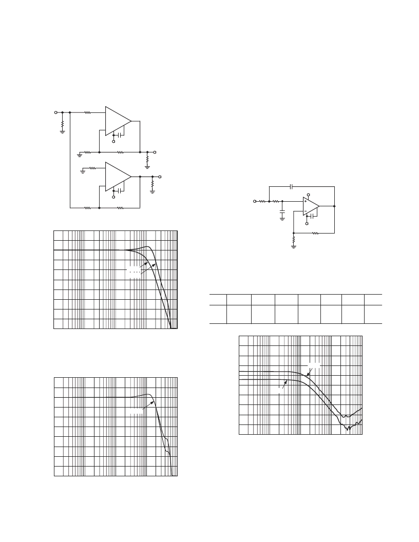
Figure 10 illustrates an inverter-follower driver circuit operating
at a gain of 2, using individually compensated AD8021s. The
values of feedback and load resistors were selected to provide a
total load of less than 1 k
, and the equivalent resistances seen
at each op amp’s inputs were matched to minimize offset volt-
age and drift. Figure 12 is a plot of the resulting ac responses of
driver halves.
AD8021
+
–
3
2
6
7pF
249
499
G = +2
499
49.9
1k
V
OUT1
5
–V
S
AD8021
+
–
3
2
6
5pF
232
G = –2
664
1k
V
OUT2
5
–V
S
332
V
IN
Figure 10. Differential Amplifier
G = –2
G = +2
G
FREQUENCY – Hz
100k
1M
10M
100M
1G
12
9
6
3
0
–3
–6
–9
–12
–15
–18
Figure 11. AC Response of Two Identically
Compensated High Speed Op Amps Configured
for Gains of +2 and –2
G = 2
100k
1M
10M
100M
1G
FREQUENCY – Hz
12
9
6
3
0
–3
–6
–9
–12
–15
–18
G
Figure12. AC Response of Two Dissimilarly
Compensated AD8021 Op Amps (Figure 11) Configured
for Gains of +2 and –2. Note the Close Gain Match.
USING THE AD8021 IN ACTIVE FILTERS
The low noise and high gain bandwidth of the AD8021 make it an
excellent choice in active filter circuits. Most active filter litera-
ture provides resistor and capacitor values for various filters but
neglects the effect of the op amp’s finite bandwidth on filter
performance; ideal filter response with infinite loop gain is implied.
Unfortunately, real filters do not behave in this manner. Instead,
they exhibit finite limits of attenuation, depending on the gain
bandwidth of the active device. Good low-pass filter performance
requires an op amp with high gain bandwidth for attenuation at
high frequencies, and low noise and high dc gain for low frequency,
pass-band performance.
Figure 13 shows the schematic of a 2-pole, low-pass active filter,
and Table IV lists typical component values for filters having a
Bessel-type response with gains of 2 and 5. Figure 14 is a network
analyzer plot of this filter’s performance.
C
C
C2
AD8021
3
2
R
F
6
V
OUT
R
G
+V
S
R2
R1
V
IN
5
–V
S
C1
Figure 13. Schematic of a Second-Order Low-Pass
Active Filter
Table IV. Typical Component Values for Second-Order
Low-Pass Filter of Figure 13
Gain
R1 ( ) R2 ( ) R
F
( ) R
S
( ) C1
71.5
215
499
44.2
365
90.9
C2
C
C
7 pF
2 pF
2
5
499
365
10 nF
10 nF
10 nF
10 nF
1k
10k
100k
1M
10M
FREQUENCY – Hz
50
40
30
20
10
0
–10
–20
–30
–40
–50
G
G = 2
G = 5
Figure 14. Frequency Response of the Filter Circuit
of Figure 13 for Two Different Gains
相關PDF資料 |
PDF描述 |
|---|---|
| AD8021AR | Low Noise, High Speed Amplifier for 16-Bit Systems |
| AD8021AR-REEL | Low Noise, High Speed Amplifier for 16-Bit Systems |
| AD8021AR-REEL7 | Low Noise, High Speed Amplifier for 16-Bit Systems |
| AD8021ARM | Low Noise, High Speed Amplifier for 16-Bit Systems |
| AD8021ARM-REEL | Low Noise, High Speed Amplifier for 16-Bit Systems |
相關代理商/技術參數 |
參數描述 |
|---|---|
| AD8021_06 | 制造商:AD 制造商全稱:Analog Devices 功能描述:Low Noise, High Speed Amplifier for 16-Bit Systems |
| AD80214ABBCZ | 制造商:Analog Devices 功能描述: |
| AD80214ABBCZRL | 功能描述:IC OP AMP 制造商:analog devices inc. 系列:* 零件狀態:上次購買時間 標準包裝:1 |
| AD80214BBCZ | 制造商:Analog Devices 功能描述: |
| AD80214BBCZRL | 制造商:Analog Devices 功能描述: |
發布緊急采購,3分鐘左右您將得到回復。