- 您現在的位置:買賣IC網 > PDF目錄373929 > AD8021ARZ (ANALOG DEVICES INC) Low Noise, High Speed Amplifier for 16-Bit Systems PDF資料下載
參數資料
| 型號: | AD8021ARZ |
| 廠商: | ANALOG DEVICES INC |
| 元件分類: | 音頻/視頻放大 |
| 英文描述: | Low Noise, High Speed Amplifier for 16-Bit Systems |
| 中文描述: | 1 CHANNEL, VIDEO AMPLIFIER, PDSO8 |
| 封裝: | LEAD FREE, MS-012AA, SOIC-8 |
| 文件頁數: | 16/20頁 |
| 文件大小: | 467K |
| 代理商: | AD8021ARZ |
REV. D
–16–
AD8021
With the AD8021, a variety of trade-offs can be made to fine-tune
its dynamic performance. Sometimes more bandwidth or slew
rate is needed at a particular gain. Reducing the compensation
capacitance, as illustrated in TPC 3, will increase the bandwidth
and peaking due to a decrease in phase margin. On the other hand,
if more stability is needed, increasing the compensation cap will
decrease the bandwidth while increasing the phase margin.
As with all high speed amplifiers, parasitic capacitance and induc-
tance around the amplifier can affect its dynamic response.
Often, the input capacitance (due to the op amp itself, as well
as the PC board) could have a significant effect. The feedback
resistance, together with the input capacitance, may contribute to
a loss of phase margin, thereby affecting the high frequency response,
as shown in TPC 10. Furthermore, a capacitor (C
F
) in parallel
with the feedback resistor can compensate for this phase loss.
Additionally, any resistance in series with the source will create
a pole with the input capacitance (as well as dampen high fre-
quency resonance due to package and board inductance and
capacitance), the effect of which is shown in TPC 11.
It must also be noted that increasing resistor values will increase
the overall noise of the amplifier, and that reducing the feedback
resistor value will increase the load on the output stage, thus
increasing distortion (TPC 18).
Using the Disable Feature
When Pin 8 (
DISABLE
) is approximately 2 V or more higher than
Pin 1 (LOGIC REFERENCE), the part is enabled. When Pin 8
is brought down to within about 1.5 V of Pin 1, the part is dis-
abled. See the Specification tables for exact disable and enable
voltage levels. If the disable feature is not going to be used, Pin 8
can be tied to V
S
or a logic high source, and Pin 1 can be tied to
ground or logic low. Alternatively, if Pin 1 and Pin 8 are not
connected, the part will be in an enabled state.
THEORY OF OPERATION
The AD8021 is fabricated on the second generation of Analog
Devices’ proprietary High Voltage eXtra-Fast Complementary
Bipolar (XFCB) process, which enables the construction of PNP
and NPN transistors with similar f
T
s in the 3 GHz region. The
transistors are dielectrically isolated from the substrate (and each
other), eliminating the parasitic and latch-up problems caused
by junction isolation. It also reduces nonlinear capacitance
(a source of distortion) and allows a higher transistor f
T
for a
given quiescent current. The supply current is trimmed, which
results in less part-to-part variation of bandwidth, slew rate,
distortion, and settling time.
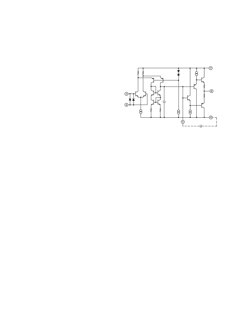
As shown in Figure 6, the AD8021 input stage consists of an NPN
differential pair in which each transistor operates at 0.8 mA collec-
tor current. This allows the input devices a high transconductance;
thus, the AD8021 has a low input noise of 2.1 nV/
√
Hz
@ 50 kHz.
The input stage drives a folded cascode that consists of a pair of
PNP transistors. The folded cascode and current mirror provide
a differential to single-ended conversion of signal current. This
current then drives the high impedance node (Pin 5), where the
C
C
external capacitor is connected. The output stage preserves
this high impedance with a current gain of 5,000, so that the
AD8021 can maintain a high open-loop gain even when driving
heavy loads.
Two internal diode clamps across the inputs (Pins 2 and 3) protect
the input transistors from large voltages that could otherwise cause
emitter-base breakdown, which would result in degradation of
offset voltage and input bias current.
C
C
OUTPUT
+V
S
–V
S
+IN
–IN
C
INTERNAL
1.5pF
C
COMP
Figure 6. Simplified Schematic
PCB LAYOUT CONSIDERATIONS
As with all high speed op amps, achieving optimum performance
from the AD8021 requires careful attention to PC board layout.
Particular care must be exercised to minimize lead lengths
between the ground leads of the bypass capacitors and between
the compensation capacitor and the negative supply. Otherwise,
lead inductance can influence the frequency response and even
cause high frequency oscillations. Use of a multilayer printed
circuit board, with an internal ground plane, will reduce ground
noise and enable a compact component arrangement.
Due to the relatively high impedance of Pin 5 and low values of
the compensation capacitor, a guard ring is recommended. The
guard ring is simply a PC trace that encircles Pin 5 and is
connected to the output, Pin 6, which is at the same potential as
Pin 5. This serves two functions. It shields Pin 5 from any local
circuit noise generated by surrounding circuitry. It also mini-
mizes stray capacitance, which would tend to otherwise reduce
the bandwidth. An example of a guard ring layout may be seen
in Figure 7.
Also shown in Figure 7, the compensation capacitor is located
immediately adjacent to the edge of the AD8021 package, spanning
Pin 4 and Pin 5. This capacitor must be a high quality surface-
mount COG or NPO ceramic. The use of leaded capacitors is not
recommended. The high frequency bypass capacitor(s) should
be located immediately adjacent to the supplies, Pins 4 and 7.
To achieve the shortest possible lead length at the inverting
input, the feedback resistor R
F
is located beneath the board and
just spans the distance from the output, Pin 6, to inverting input
Pin 2. The return node of resistor R
G
should be situated as
closely as possible to the return node of the negative supply
bypass capacitor connected to Pin 4.
相關PDF資料 |
PDF描述 |
|---|---|
| AD8021ARZ-REEL7 | Low Noise, High Speed Amplifier for 16-Bit Systems |
| AD8021ARZ-REEL | Low Noise, High Speed Amplifier for 16-Bit Systems |
| AD8023ACHIPS | High Current Output, Triple Video Amplifier |
| AD8023AR | High Current Output, Triple Video Amplifier |
| AD8023AR-REEL7 | High Current Output, Triple Video Amplifier |
相關代理商/技術參數 |
參數描述 |
|---|---|
| AD8021ARZ-REEL | 功能描述:IC OPAMP VF LN LP LDIST 8SOIC RoHS:是 類別:集成電路 (IC) >> Linear - Amplifiers - Instrumentation 系列:- 標準包裝:1,000 系列:- 放大器類型:電壓反饋 電路數:4 輸出類型:滿擺幅 轉換速率:33 V/µs 增益帶寬積:20MHz -3db帶寬:30MHz 電流 - 輸入偏壓:2nA 電壓 - 輸入偏移:3000µV 電流 - 電源:2.5mA 電流 - 輸出 / 通道:30mA 電壓 - 電源,單路/雙路(±):4.5 V ~ 16.5 V,±2.25 V ~ 8.25 V 工作溫度:-40°C ~ 85°C 安裝類型:表面貼裝 封裝/外殼:14-SOIC(0.154",3.90mm 寬) 供應商設備封裝:14-SOIC 包裝:帶卷 (TR) |
| AD8021ARZ-REEL7 | 功能描述:IC OPAMP VF LN LP LDIST 8SOIC RoHS:是 類別:集成電路 (IC) >> Linear - Amplifiers - Instrumentation 系列:- 產品培訓模塊:Differential Circuit Design Techniques for Communication Applications 標準包裝:1 系列:- 放大器類型:RF/IF 差分 電路數:1 輸出類型:差分 轉換速率:9800 V/µs 增益帶寬積:- -3db帶寬:2.9GHz 電流 - 輸入偏壓:3µA 電壓 - 輸入偏移:- 電流 - 電源:40mA 電流 - 輸出 / 通道:- 電壓 - 電源,單路/雙路(±):3 V ~ 3.6 V 工作溫度:-40°C ~ 85°C 安裝類型:表面貼裝 封裝/外殼:16-VQFN 裸露焊盤,CSP 供應商設備封裝:16-LFCSP-VQ 包裝:剪切帶 (CT) 產品目錄頁面:551 (CN2011-ZH PDF) 其它名稱:ADL5561ACPZ-R7CT |
| AD8022 | 制造商:未知廠家 制造商全稱:未知廠家 功能描述:AD8022: Dual High-Speed Low-Noise Op Amps Data Sheet (Rev. A. 9/02) |
| AD8022_05 | 制造商:AD 制造商全稱:Analog Devices 功能描述:Dual High Speed, Low Noise Op Amp |
| AD80220BBCZ | 制造商:Analog Devices 功能描述: |
發布緊急采購,3分鐘左右您將得到回復。