- 您現在的位置:買賣IC網 > PDF目錄373929 > AD8027ART-REEL (ANALOG DEVICES INC) Low Distortion, High Speed Rail-to-Rail Input/Output Amplifiers PDF資料下載
參數資料
| 型號: | AD8027ART-REEL |
| 廠商: | ANALOG DEVICES INC |
| 元件分類: | 音頻/視頻放大 |
| 英文描述: | Low Distortion, High Speed Rail-to-Rail Input/Output Amplifiers |
| 中文描述: | 1 CHANNEL, VIDEO AMPLIFIER, PDSO6 |
| 封裝: | MO-178AB, SOT-23, 6 PIN |
| 文件頁數: | 19/24頁 |
| 文件大小: | 478K |
| 代理商: | AD8027ART-REEL |
AD8027/AD8028
Circuit Considerations
Rev. B | Page 19 of 24
BALANCED INPUT IMPEDANCES
Balanced input impedances can help improve distortion per-
formance. When the amplifier transitions from PNP pair to
NPN pair operation, a change in both the magnitude and direc-
tion of the input bias current will occur. When multiplied times
imbalanced input impedances, a change in offset will result. The
key to minimizing this distortion is to keep the input imped-
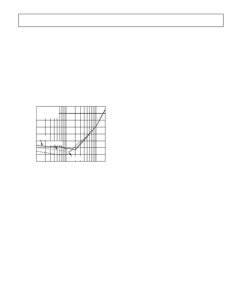
ances balanced on both inputs. Figure 59 shows the effect of the
imbalance and degradation in distortion performance for a
50 source impedance, with and without a 50 balanced feed-
back path.
FREQUENCY (MHz)
0.1
1
10
20
D
–100
–90
–80
–70
–60
–50
–40
–30
–20
G = +1
V
OUT
= 2V p-p
R
L
V
S
= +3V
R
F
= 24.9
R
F
= 49.9
R
F
= 0
03327-A-058
Figure 59. SFDR vs. Frequency and Various R
F
PCB LAYOUT
As with all high speed op amps, achieving optimum perform-
ance from the AD8027/AD8028 requires careful attention to
PCB layout. Particular care must be exercised to minimize lead
lengths of the bypass capacitors. Excess lead inductance can
influence the frequency response and even cause high fre-
quency oscillations. The use of a multilayer board, with an
internal ground plane, will reduce ground noise and enable a
tighter layout.
To achieve the shortest possible lead length at the inverting
input, the feedback resistor, R
F
,
should be located beneath the
board and span the distance from the output, Pin 6, to the input,
Pin 2. The return node of the resistor R
G
should be situated as
closely as possible to the return node of the negative supply
bypass capacitor connected to Pin 4.
On multilayer boards, all layers underneath the op amp should
be cleared of metal to avoid creating parasitic capacitive
elements. This is especially true at the summing junction (i.e.,
the –input). Extra capacitance at the summing junction can
cause increased peaking in the frequency response and lower
phase margin.
GROUNDING
To minimize parasitic inductances and ground loops in high
speed, densely populated boards, a ground plane layer is critical.
Understanding where the current flows in a circuit is critical in
the implementation of high speed circuit design. The length of
the current path is directly proportional to the magnitude of the
parasitic inductances and thus the high frequency impedance of
the path. Fast current changes in an inductive ground return
will create unwanted noise and ringing.
The length of the high frequency bypass capacitor pads and
traces is critical. A parasitic inductance in the bypass grounding
will work against the low impedance created by the bypass
capacitor. Because load currents flow from supplies as well as
ground, the load should be placed at the same physical location
as the bypass capacitor ground. For large values of capacitors,
which are intended to be effective at lower frequencies, the cur-
rent return path length is less critical.
POWER SUPPLY BYPASSING
Power supply pins are actually inputs and care must be taken to
provide a clean, low noise dc voltage source to these inputs. The
bypass capacitors have two functions:
1.
Provide a low impedance path for unwanted frequencies
from the supply inputs to ground, thereby reducing the
effect of noise on the supply lines.
2.
Provide sufficient localized charge storage, for fast
switching conditions and minimizing the voltage drop at
the supply pins and the output of the amplifier. This is
usually accomplished with larger electrolytic capacitors.
Decoupling methods are designed to minimize the bypassing
impedance at all frequencies. This can be accomplished with a
combination of capacitors in parallel to ground.
Good quality ceramic chip capacitors should be used and
always kept as close to the amplifier package as possible. A par-
allel combination of a 0.01 μF ceramic and a 10 μF electrolytic
covers a wide range of rejection for unwanted noise. The 10 μF
capacitor is less critical for high frequency bypassing, and in
most cases, one per supply line is sufficient.
相關PDF資料 |
PDF描述 |
|---|---|
| AD8027ART-REEL7 | Low Distortion, High Speed Rail-to-Rail Input/Output Amplifiers |
| AD8028AR | Low Distortion, High Speed Rail-to-Rail Input/Output Amplifiers |
| AD8028AR-REEL | Low Distortion, High Speed Rail-to-Rail Input/Output Amplifiers |
| AD8028AR-REEL7 | Low Distortion, High Speed Rail-to-Rail Input/Output Amplifiers |
| AD8028ARM | Low Distortion, High Speed Rail-to-Rail Input/Output Amplifiers |
相關代理商/技術參數 |
參數描述 |
|---|---|
| AD8027ART-REEL7 | 功能描述:IC OPAMP R-R LDIST LN LP SOT23-6 RoHS:否 類別:集成電路 (IC) >> Linear - Amplifiers - Instrumentation 系列:- 標準包裝:2,500 系列:- 放大器類型:通用 電路數:1 輸出類型:滿擺幅 轉換速率:0.11 V/µs 增益帶寬積:350kHz -3db帶寬:- 電流 - 輸入偏壓:4nA 電壓 - 輸入偏移:20µV 電流 - 電源:260µA 電流 - 輸出 / 通道:20mA 電壓 - 電源,單路/雙路(±):2.7 V ~ 36 V,±1.35 V ~ 18 V 工作溫度:-40°C ~ 85°C 安裝類型:表面貼裝 封裝/外殼:8-SOIC(0.154",3.90mm 寬) 供應商設備封裝:8-SO 包裝:帶卷 (TR) |
| AD8027ARTZ | 制造商:Analog Devices 功能描述:OP AMP R-R LDIST LN LP SOT23-6 制造商:Analog Devices 功能描述:OP AMP, R-R, LDIST, LN, LP, SOT23-6 制造商:Analog Devices 功能描述:OP AMP, R-R, LDIST, LN, LP, SOT23-6; Op Amp Type:Rail to Rail; No. of Amplifiers:1; Slew Rate:100V/s; Supply Voltage Range:2.7V to 12V; Amplifier Case Style:SOT-23; No. of Pins:6; Bandwidth:190MHz; Operating Temperature Min:-40C; ;RoHS Compliant: Yes 制造商:Analog Devices 功能描述:Amplifier,Op-Amp,V feedback,AD8027ARTZ |
| AD8027ARTZ-R2 | 功能描述:IC OPAMP R-R LDIST LN LP SOT23-6 RoHS:是 類別:集成電路 (IC) >> Linear - Amplifiers - Instrumentation 系列:- 標準包裝:2,500 系列:- 放大器類型:通用 電路數:1 輸出類型:滿擺幅 轉換速率:0.11 V/µs 增益帶寬積:350kHz -3db帶寬:- 電流 - 輸入偏壓:4nA 電壓 - 輸入偏移:20µV 電流 - 電源:260µA 電流 - 輸出 / 通道:20mA 電壓 - 電源,單路/雙路(±):2.7 V ~ 36 V,±1.35 V ~ 18 V 工作溫度:-40°C ~ 85°C 安裝類型:表面貼裝 封裝/外殼:8-SOIC(0.154",3.90mm 寬) 供應商設備封裝:8-SO 包裝:帶卷 (TR) |
| AD8027ARTZ-REEL | 功能描述:IC OPAMP R-R LDIST LN LP SOT23-6 RoHS:是 類別:集成電路 (IC) >> Linear - Amplifiers - Instrumentation 系列:- 標準包裝:2,500 系列:- 放大器類型:通用 電路數:1 輸出類型:滿擺幅 轉換速率:0.11 V/µs 增益帶寬積:350kHz -3db帶寬:- 電流 - 輸入偏壓:4nA 電壓 - 輸入偏移:20µV 電流 - 電源:260µA 電流 - 輸出 / 通道:20mA 電壓 - 電源,單路/雙路(±):2.7 V ~ 36 V,±1.35 V ~ 18 V 工作溫度:-40°C ~ 85°C 安裝類型:表面貼裝 封裝/外殼:8-SOIC(0.154",3.90mm 寬) 供應商設備封裝:8-SO 包裝:帶卷 (TR) |
| AD8027ARTZ-REEL7 | 功能描述:IC OPAMP R-R LDIST LN LP SOT23-6 RoHS:是 類別:集成電路 (IC) >> Linear - Amplifiers - Instrumentation 系列:- 產品培訓模塊:Differential Circuit Design Techniques for Communication Applications 標準包裝:1 系列:- 放大器類型:RF/IF 差分 電路數:1 輸出類型:差分 轉換速率:9800 V/µs 增益帶寬積:- -3db帶寬:2.9GHz 電流 - 輸入偏壓:3µA 電壓 - 輸入偏移:- 電流 - 電源:40mA 電流 - 輸出 / 通道:- 電壓 - 電源,單路/雙路(±):3 V ~ 3.6 V 工作溫度:-40°C ~ 85°C 安裝類型:表面貼裝 封裝/外殼:16-VQFN 裸露焊盤,CSP 供應商設備封裝:16-LFCSP-VQ 包裝:剪切帶 (CT) 產品目錄頁面:551 (CN2011-ZH PDF) 其它名稱:ADL5561ACPZ-R7CT |
發布緊急采購,3分鐘左右您將得到回復。