- 您現(xiàn)在的位置:買賣IC網(wǎng) > PDF目錄373931 > AD8033AR-REEL7 (ANALOG DEVICES INC) Low Cost, 80 MHz FastFET ⑩ Op Amps PDF資料下載
參數(shù)資料
| 型號(hào): | AD8033AR-REEL7 |
| 廠商: | ANALOG DEVICES INC |
| 元件分類: | 運(yùn)動(dòng)控制電子 |
| 英文描述: | Low Cost, 80 MHz FastFET ⑩ Op Amps |
| 中文描述: | OP-AMP, 3500 uV OFFSET-MAX, PDSO8 |
| 封裝: | MS-012AA, SOIC-8 |
| 文件頁數(shù): | 15/20頁 |
| 文件大小: | 374K |
| 代理商: | AD8033AR-REEL7 |
REV. B
AD8033/AD8034
–15–
LAYOUT, GROUNDING, AND BYPASSING
CONSIDERATIONS
Bypassing
Power supply pins are actually inputs, and care must be taken
so that a noise-free stable dc voltage is applied. The purpose of
bypass capacitors is to create low impedances from the supply to
ground at all frequencies, thereby shunting or filtering a majority
of the noise. Decoupling schemes are designed to minimize the
bypassing impedance at all frequencies with a parallel combination
of capacitors. 0.01
μ
F or 0.001
μ
F (X7R or NPO) chip capacitors
are critical and should be placed as close as possible to the
amplifier package. Larger chip capacitors, such as the 0.1
μ
F
capacitor, can be shared among a few closely spaced active
components in the same signal path. The 10
μ
F tantalum capacitor
is less critical for high frequency bypassing, and in most cases,
only one per board is needed at the supply inputs.
Grounding
A ground plane layer is important in densely packed PC boards
in
order to spread the current, thereby minimizing parasitic induc-
tances. However,
an understanding of where the current flows in
a circuit is critical
to implementing effective high speed circuit
design. The length of the current path is directly proportional to
the magnitude of
the parasitic inductances, and thus the high
frequency impedance
of the path. High speed currents in an
inductive ground return will
create unwanted voltage noise. The
length of the high frequency
bypass capacitor leads is most critical.
A parasitic inductance in the bypass grounding will work against
the low impedance created by the bypass capacitor. Place the
ground leads of the bypass capacitors at the same physical location.
Because load currents flow from the supplies as well, the ground
for the load impedance should be at the same physical location
as the bypass capacitor grounds. For the larger value capacitors
that are intended to be effective at lower frequencies, the current
return path distance is less critical.
Leakage Currents
Poor PC board layout, contaminants, and the board insulator
material can create leakage currents that are much larger than the
input bias currents of the
AD8033/AD8034
. Any voltage differen
tial
between the inputs and nearby runs will set up leakage
currents
through the PC board insulator, for example, 1 V/100 G
= 10 pA.
Similarly, any contaminants on the board can create significant
leakage (skin oils are a common problem).
To significantly reduce
leakages, put a guard ring (shield) around
the inputs and input
leads that are driven to the same voltage potential as the
inputs.
This way there is no voltage potential between the inputs
and
surrounding area to set up any leakage currents. For the guard
ring
to be completely effective, it must be driven by a relatively low
impedance source and should
completely surround the input
leads on all sides, above, and below
using a multilayer board.
Another effect that can cause leakage currents is the charge
absorption of the insulator material itself. Minimizing the amount
of material between the
input leads and the guard ring will help
to reduce the absorption.
Also, low absorption materials such as
Teflon
or ceramic may be necessary in some instances.
Input Capacitance
Along with bypassing and ground, high speed amplifiers can be
sensitive to parasitic capacitance between the inputs and ground.
A few pF of capacitance will reduce the input impedance at high
frequencies, in turn increasing the amplifiers’ gain and causing
peaking
of the overall response or even oscillations if severe
enough. It is recommended that the external passive components
that are connected to the input pins be placed as close as possible
to the inputs to avoid parasitic capacitance. The ground and power
planes must be kept at a distance of at least 0.05 mm from the
input pins on all layers of the board.
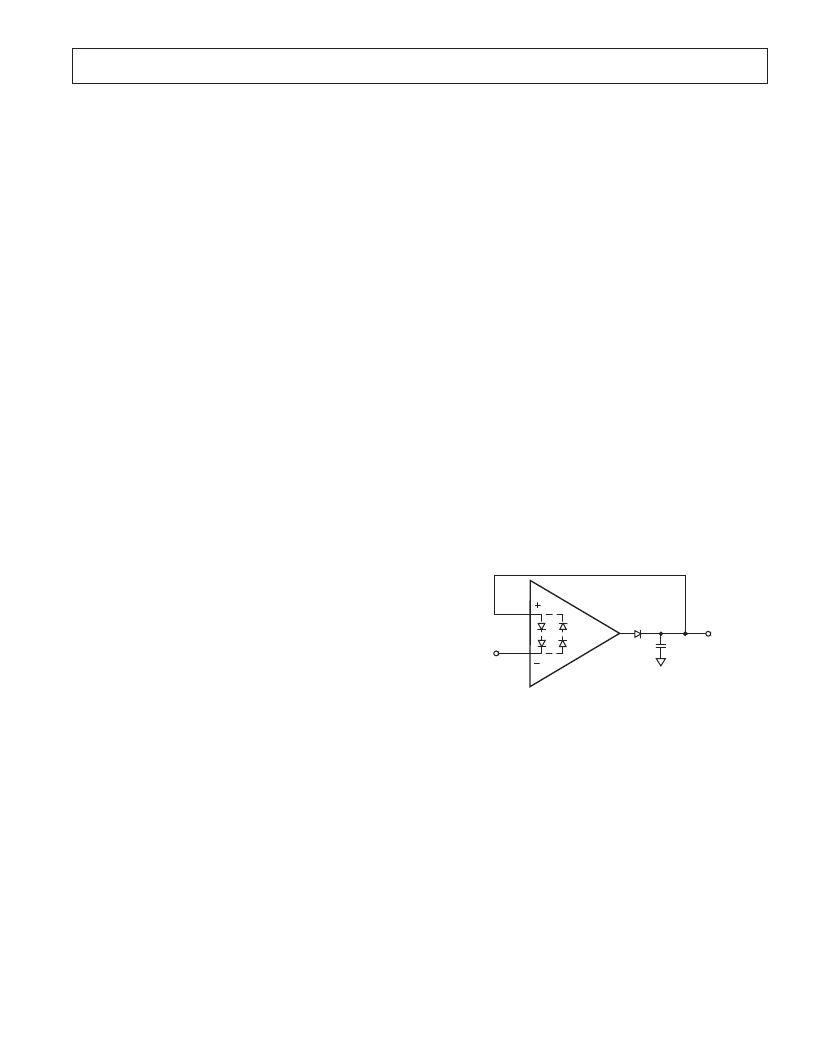
APPLICATIONS
High Speed Peak Detector
The low input bias current and high bandwidth of the AD8033/
AD8034 make the parts ideal for a fast settling, low leakage peak
detector. The classic fast-low leakage topology with a diode in
the output is limited to 1.4 V p-p max in the case of the
AD8033/AD8034 because of the protection diodes across the
inputs, as depicted in Figure 4.
AD8033/
AD8034
V
IN
~1.4V p-p MAX
V
OUT
Figure 4. High Speed Peak Detector with Limited Input Range
相關(guān)PDF資料 |
PDF描述 |
|---|---|
| AD8034 | Low Cost, 80 MHz FastFET ⑩ Op Amps |
| AD8034AR | Low Cost, 80 MHz FastFET ⑩ Op Amps |
| AD8034AR-REEL | Low Cost, 80 MHz FastFET ⑩ Op Amps |
| AD8034AR-REEL7 | Low Cost, 80 MHz FastFET ⑩ Op Amps |
| AD8034ART-REEL | Low Cost, 80 MHz FastFET ⑩ Op Amps |
相關(guān)代理商/技術(shù)參數(shù) |
參數(shù)描述 |
|---|---|
| AD8033ARZ | 功能描述:IC OPAMP VF R-R LN LP 60MA 8SOIC RoHS:是 類別:集成電路 (IC) >> Linear - Amplifiers - Instrumentation 系列:FastFET™ 產(chǎn)品培訓(xùn)模塊:Differential Circuit Design Techniques for Communication Applications 標(biāo)準(zhǔn)包裝:1 系列:- 放大器類型:RF/IF 差分 電路數(shù):1 輸出類型:差分 轉(zhuǎn)換速率:9800 V/µs 增益帶寬積:- -3db帶寬:2.9GHz 電流 - 輸入偏壓:3µA 電壓 - 輸入偏移:- 電流 - 電源:40mA 電流 - 輸出 / 通道:- 電壓 - 電源,單路/雙路(±):3 V ~ 3.6 V 工作溫度:-40°C ~ 85°C 安裝類型:表面貼裝 封裝/外殼:16-VQFN 裸露焊盤,CSP 供應(yīng)商設(shè)備封裝:16-LFCSP-VQ 包裝:剪切帶 (CT) 產(chǎn)品目錄頁面:551 (CN2011-ZH PDF) 其它名稱:ADL5561ACPZ-R7CT |
| AD8033ARZ | 制造商:Analog Devices 功能描述:OP AMP FAST FET SMD 8033 SOIC8 |
| AD8033ARZ1 | 制造商:AD 制造商全稱:Analog Devices 功能描述:Low Cost, 80 MHz FastFET Op Amps |
| AD8033ARZ-REEL | 功能描述:IC OPAMP VF R-R LN LP 60MA 8SOIC RoHS:是 類別:集成電路 (IC) >> Linear - Amplifiers - Instrumentation 系列:FastFET™ 標(biāo)準(zhǔn)包裝:2,500 系列:- 放大器類型:通用 電路數(shù):1 輸出類型:滿擺幅 轉(zhuǎn)換速率:0.11 V/µs 增益帶寬積:350kHz -3db帶寬:- 電流 - 輸入偏壓:4nA 電壓 - 輸入偏移:20µV 電流 - 電源:260µA 電流 - 輸出 / 通道:20mA 電壓 - 電源,單路/雙路(±):2.7 V ~ 36 V,±1.35 V ~ 18 V 工作溫度:-40°C ~ 85°C 安裝類型:表面貼裝 封裝/外殼:8-SOIC(0.154",3.90mm 寬) 供應(yīng)商設(shè)備封裝:8-SO 包裝:帶卷 (TR) |
| AD8033ARZ-REEL7 | 功能描述:IC OPAMP VF R-R LN LP 60MA 8SOIC RoHS:是 類別:集成電路 (IC) >> Linear - Amplifiers - Instrumentation 系列:FastFET™ 標(biāo)準(zhǔn)包裝:2,500 系列:- 放大器類型:通用 電路數(shù):1 輸出類型:滿擺幅 轉(zhuǎn)換速率:0.11 V/µs 增益帶寬積:350kHz -3db帶寬:- 電流 - 輸入偏壓:4nA 電壓 - 輸入偏移:20µV 電流 - 電源:260µA 電流 - 輸出 / 通道:20mA 電壓 - 電源,單路/雙路(±):2.7 V ~ 36 V,±1.35 V ~ 18 V 工作溫度:-40°C ~ 85°C 安裝類型:表面貼裝 封裝/外殼:8-SOIC(0.154",3.90mm 寬) 供應(yīng)商設(shè)備封裝:8-SO 包裝:帶卷 (TR) |
發(fā)布緊急采購,3分鐘左右您將得到回復(fù)。