- 您現在的位置:買賣IC網 > PDF目錄373931 > AD8037 (Analog Devices, Inc.) Low Distortion, Wide Bandwidth Voltage Feedback Clamp Amps(低失真,寬帶電壓反饋鉗位放大器) PDF資料下載
參數資料
| 型號: | AD8037 |
| 廠商: | Analog Devices, Inc. |
| 英文描述: | Low Distortion, Wide Bandwidth Voltage Feedback Clamp Amps(低失真,寬帶電壓反饋鉗位放大器) |
| 中文描述: | 低失真,寬帶電壓反饋鉗放大器(低失真,寬帶電壓反饋鉗位放大器) |
| 文件頁數: | 18/24頁 |
| 文件大小: | 585K |
| 代理商: | AD8037 |
REV. 0
–18–
AD8036/AD8037
The analog input range of the AD9002 is from ground to –2 V.
The input should not go more than 0.5 V outside this range in
order to prevent disruptions to the internal workings of the A/D
and to avoid drawing excess current. These requirements make
the AD8037 a prime candidate for signal conditioning.
When an offset is added to a noninverting op amp circuit, it is
fed in through a resistor to the inverting input. The result is that
the op amp must now operate at a closed-loop gain greater than
unity. For this circuit a gain of two was chosen which allows the
use of the AD8037. The feedback resistor, R2, is set at 301
for optimum performance of the AD8037 at a gain of two.
There is an interaction between the offset and the gain, so some
calculations must be performed to arrive at the proper values for
R1 and R3. For a gain of two the parallel combination of resis-
tors R1 and R3 must be equal to the feedback resistor R2. Thus
R
1
×
R
3/
R
1 +
R
3 =
R
2 = 301
The reference used to provide the offset is the AD780 whose
output is 2.5 V. This must be divided down to provide the 1 V
offset desired. Thus
2.5
V
×
R
1/(
R
1 +
R
3) = 1 V
When the two equations are solved simultaneously we get R1 =
499
and R3 = 750
(using closest 1% resistor values in all
cases). This positive 1 V offset at the input translates to a –1 V
offset at the output.
The usable input signal swing of the AD9002 is 2 V p-p. This is
centered about the –1 V offset making the usable signal range
from 0 V to –2 V. It is desirable to clamp the input signal so
that it goes no more than 100 mV outside of this range in either
direction. Thus, the high clamping level should be set at +0.1 V
and the low clamping level should be set at –2.1 V as seen at the
input of the AD9002 (output of AD8037).
Because the clamping is done at the input stage of the AD8037,
the clamping level as seen at the output is affected by not only
the gain of the circuit as previously described, but also by the
offset. Thus, in order to obtain the desired clamp levels, V
H
must be biased at +0.55 V while V
L
must be biased at –0.55 V.
The clamping levels as seen at the output can be calculated by
the following:
V
CH
=
V
OFF
+
G
×
V
H
V
CL
=
V
OFF
+
G
×
V
L
Where V
OFF
is the offset voltage that appears at the output.
The resistors used to generate the voltages for V
H
and V
L
should
be kept to a minimum in order to reduce errors due to clamp
bias current. This current is dependent on V
H
and V
L
(see Fig-
ure 61) and will create a voltage drop across whatever resistance
is in series with each clamp input. This extra error voltage is
multiplied by the closed-loop gain of the amplifier and can be
substantial, especially in high closed-loop gain configurations. A
0.1
μ
F bypass capacitor should be placed between input clamp
pins V
H
and V
L
and ground to ensure stable operation.
The 1N5712 Schottky diode is used for protection from forward
biasing the substrate diode in the AD9002 during power-up
transients.
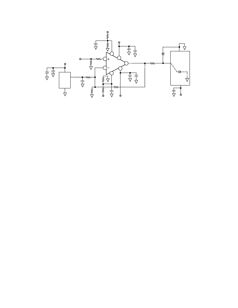
Programmable Pulse Generator
The AD8036/AD8037’s clamp output can be set accurately and
has a well controlled flat level. This along with wide bandwidth
and high slew rate make them very well suited for programmable
level pulse generators.
Figure 77 is a schematic for a pulse generator that can directly
accept TTL generated timing signals for its input and generate
pulses at the output up to 24 V p-p with 2500 V/
μ
s slew rate.
The output levels can be programmed to anywhere in the range
–12 V to +12 V.
The circuit uses an AD8037 operating at a gain of two with an
AD811 to boost the output to the
±
12 V range. The AD811 was
chosen for its ability to operate with
±
15 V supplies and its high
slew rate.
R1 and R2 act as a level shifter to make the TTL signal levels be
approximately symmetrical above and below ground. This en-
sures that both the high and low logic levels will be clamped by
the AD8037. For well controlled signal levels in the output
pulse, the high and low output levels should result from the
clamping action of the AD8037 and not be controlled by either
+5V
V
IN
R2
100
AD8037
3
6
7
4
8
5
–5V
+
+
301
V
L
2
V
H
GAIN OF TWO, NONINVERTING WITH OFFSET AD8037
DRIVING AN AD9002 – 8-BIT, 125 MSPS A/D CONVERTER
806
100
+5V
49.9
750
–0.5V to +0.5V
0.1μF
0.1μF
10μF
R3
100
0.1
μF
806
–5V
49.9
–2V to 0V
CLAMPING
RANGE
–2.1V to +0.1V
499
R1
0.1
μF
2.5V
AD780
+5V
+
0.1
μF
10μF
AD9002
VIN= –2V TO 0V
SUBSTRATE
DIODE
–5.2V
0.1μF
1N5712
0.1μF
10μF
Figure 76. Gain of Two, Noninverting with Offset AD8037 Driving an AD9002—8-Bit, 125 MSPS A/D Converter
相關PDF資料 |
PDF描述 |
|---|---|
| AD8037AR-REEL7 | Low Distortion, Wide Bandwidth Voltage Feedback Clamp Amps |
| AD8036-EB | Low Distortion, Wide Bandwidth Voltage Feedback Clamp Amps |
| AD8037ACHIPS | Connector assemblies, Test RoHS Compliant: Yes |
| AD8037AN | Low Distortion, Wide Bandwidth Voltage Feedback Clamp Amps |
| AD8037AR | Low Distortion, Wide Bandwidth Voltage Feedback Clamp Amps |
相關代理商/技術參數 |
參數描述 |
|---|---|
| AD8037ACHIPS | 制造商:AD 制造商全稱:Analog Devices 功能描述:Low Distortion, Wide Bandwidth Voltage Feedback Clamp Amps |
| AD8037AN | 制造商:Analog Devices 功能描述:OP Amp Single Volt Fdbk ±6V 8-Pin PDIP 制造商:Rochester Electronics LLC 功能描述:VLTG-FDBK, G= 2 CLAMP AMP - Bulk 制造商:Analog Devices 功能描述:IC AMP 240MHZ CLAMP 8037 DIP8 |
| AD8037ANZ | 功能描述:IC OPAMP VF ULDIST LN 70MA 8DIP RoHS:是 類別:集成電路 (IC) >> Linear - Amplifiers - Instrumentation 系列:CLAMPIN™ 標準包裝:1 系列:- 放大器類型:通用 電路數:4 輸出類型:滿擺幅 轉換速率:0.028 V/µs 增益帶寬積:105kHz -3db帶寬:- 電流 - 輸入偏壓:3nA 電壓 - 輸入偏移:100µV 電流 - 電源:3.3µA 電流 - 輸出 / 通道:12mA 電壓 - 電源,單路/雙路(±):2.7 V ~ 12 V,±1.35 V ~ 6 V 工作溫度:-40°C ~ 85°C 安裝類型:表面貼裝 封裝/外殼:14-TSSOP(0.173",4.40mm 寬) 供應商設備封裝:14-TSSOP 包裝:剪切帶 (CT) 其它名稱:OP481GRUZ-REELCT |
| AD8037AR | 功能描述:IC OPAMP VF ULDIST LN 70MA 8SOIC RoHS:否 類別:集成電路 (IC) >> Linear - Amplifiers - Instrumentation 系列:CLAMPIN™ 標準包裝:2,500 系列:Excalibur™ 放大器類型:J-FET 電路數:1 輸出類型:- 轉換速率:45 V/µs 增益帶寬積:10MHz -3db帶寬:- 電流 - 輸入偏壓:20pA 電壓 - 輸入偏移:490µV 電流 - 電源:1.7mA 電流 - 輸出 / 通道:48mA 電壓 - 電源,單路/雙路(±):4.5 V ~ 38 V,±2.25 V ~ 19 V 工作溫度:-40°C ~ 85°C 安裝類型:表面貼裝 封裝/外殼:8-SOIC(0.154",3.90mm 寬) 供應商設備封裝:8-SOIC 包裝:帶卷 (TR) |
| AD8037AR-REEL | 制造商:Analog Devices 功能描述:OP Amp Single Volt Fdbk 制造商:Analog Devices 功能描述:OP Amp Single Volt Fdbk ±6V 8-Pin SOIC N T/R 制造商:Rochester Electronics LLC 功能描述:VLTG-FDBK, G= 2 CLAMP AMP - Tape and Reel |
發布緊急采購,3分鐘左右您將得到回復。