- 您現在的位置:買賣IC網 > PDF目錄373931 > AD8037AR (ANALOG DEVICES INC) Low Distortion, Wide Bandwidth Voltage Feedback Clamp Amps PDF資料下載
參數資料
| 型號: | AD8037AR |
| 廠商: | ANALOG DEVICES INC |
| 元件分類: | 運動控制電子 |
| 英文描述: | Low Distortion, Wide Bandwidth Voltage Feedback Clamp Amps |
| 中文描述: | OP-AMP, 10000 uV OFFSET-MAX, PDSO8 |
| 封裝: | SOIC-8 |
| 文件頁數: | 16/23頁 |
| 文件大小: | 387K |
| 代理商: | AD8037AR |
REV. A
–16–
AD8036/AD8037
Operation of the AD8036 for negative input voltages and nega-
tive clamp levels on V
L
is similar, with comparator C
L
control-
ling S1. Since the comparators see the voltage on the +V
IN
pin
as their common reference level, then the voltage V
H
and V
L
are
defined as “High” or “Low” with respect to +V
IN
. For example,
if V
IN
is set to zero volts, V
H
is open, and V
L
is +1 V, compara-
tor C
L
will switch S1 to “C,” so the AD8036 will buffer the
voltage on V
L
and ignore +V
IN
.
The performance of the AD8036 and AD8037 closely matches
the ideal just described. The comparator’s threshold extends
from 60 mV inside the clamp window defined by the voltages on
V
L
and V
H
to 60 mV beyond the window’s edge. Switch S1 is
implemented with current steering, so that A1’s +input makes a
continuous transition from say, V
IN
to V
H
as the input voltage
traverses the comparator’s input threshold from 0.9 V to 1.0 V
for V
H
= 1.0 V.
The practical effect of these nonidealities is to soften the
transition from amplification to clamping modes, without com-
promising the absolute clamp limit set by the CLAMPIN cir-
cuit. Figure 73 is a graph of V
OUT
vs. V
IN
for the AD8036 and a
typical output clamp amplifier. Both amplifiers are set for G =
+1 and V
H
= +1 V.
The worst case error between V
OUT
(ideally clamped) and V
OUT
(actual) is typically 18 mV times the amplifier closed-loop gain.
This occurs when V
IN
equals V
H
(or V
L
). As V
IN
goes above
and/or below this limit, V
OUT
will settle to within 5 mV of the
ideal value.
In contrast, the output clamp amplifier’s transfer curve typically
will show some compression starting at an input of 0.8 V, and
can have an output voltage as far as 200 mV over the clamp
limit. In addition, since the output clamp in effect causes the
amplifier to operate open loop in clamp mode, the amplifier’s
output impedance will increase, potentially causing additional
errors.
The AD8036’s and AD8037’s CLAMPIN input clamp architec-
ture works only for noninverting or follower applications and,
since it operates on the input, the clamp voltage levels V
H
and
V
L
, and input error limits will be multiplied by the amplifier’s
A
B
C
S1
R
F
140
V
A B C
0 1 0
1 0 0
0 0 1
S1
V
IN
> V
H
V
L
≤
V
IN
≤
V
H
V
IN
< V
L
–V
IN
+V
IN
V
H
V
L
V
OUT
+1
+1
+1
C
H
C
L
A1
A2
+1
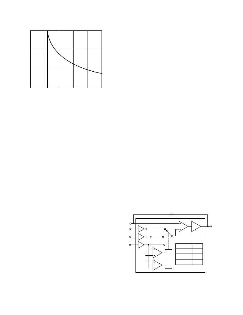
Figure 72. AD8036/AD8037 Clamp Amp System
0 5 10 15 20 25
C
L
– pF
R
S
V
40
30
20
10
Figure 71. Recommended R
SERIES
vs. Capacitive Load
INPUT CLAMPING AMPLIFIER OPERATION
The key to the AD8036 and AD8037’s fast, accurate clamp and
amplifier performance is their unique patent pending CLAMPIN
input clamp architecture. This new design reduces clamp errors
by more than 10
×
over previous output clamp based circuits, as
well as substantially increasing the bandwidth, precision and
versatility of the clamp inputs.
Figure 72 is an idealized block diagram of the AD8036 con-
nected as a unity gain voltage follower. The primary signal path
comprises A1 (a 1200 V/
μ
s, 240 MHz high voltage gain, differ-
ential to single-ended amplifier) and A2 (a G = +1 high current
gain output buffer). The AD8037 differs from the AD8036 only
in that A1 is optimized for closed-loop gains of two or greater.
The CLAMPIN section is comprised of comparators C
H
and
C
L
, which drive switch S1 through a decoder. The unity-gain
buffers in series with +V
IN
, V
H
, and V
L
inputs isolate the input
pins from the comparators and S1 without reducing bandwidth
or precision.
The two comparators have about the same bandwidth as A1
(240 MHz), so they can keep up with signals within the useful
bandwidth of the AD8036. To illustrate the operation of the
CLAMPIN circuit, consider the case where V
H
is referenced to
+1 V, V
L
is open, and the AD8036 is set for a gain of +1, by
connecting its output back to its inverting input through the rec-
ommended 140
feedback resistor. Note that the main signal
path always operates closed loop, since the CLAMPIN circuit
only affects A1’s noninverting input.
If a 0 V to +2 V voltage ramp is applied to the AD8036’s +V
IN
for the connection just described, V
OUT
should track +V
IN
per-
fectly up to +1 V, then should limit at exactly +1 V as +V
IN
con-
tinues to +2 V.
In practice, the AD8036 comes close to this ideal behavior. As
the +V
IN
input voltage ramps from zero to 1 V, the output of the
high limit comparator C
H
starts in the off state, as does the out-
put of C
L
. When +V
IN
just exceeds V
IN
(ideally, by say 1
μ
V,
practically by about 18 mV), C
H
changes state, switching S1
from “A” to “B” reference level. Since the + input of A1 is now
connected to V
H
, further increases in +V
IN
have no effect on the
AD8036’s output voltage. In short, the AD8036 is now operat-
ing as a unity-gain buffer for the V
H
input, as any variation in
V
H
, for V
H
> 1 V, will be faithfully reproduced at V
OUT
.
相關PDF資料 |
PDF描述 |
|---|---|
| AD8036ACHIPS | Low Distortion, Wide Bandwidth Voltage Feedback Clamp Amps |
| AD8036AN | Low Distortion, Wide Bandwidth Voltage Feedback Clamp Amps |
| AD8036AR | Low Distortion, Wide Bandwidth Voltage Feedback Clamp Amps |
| AD8037-EB | MB 26C 26#20 PIN PLUG |
| AD8036AR-REEL | Low Distortion, Wide Bandwidth Voltage Feedback Clamp Amps |
相關代理商/技術參數 |
參數描述 |
|---|---|
| AD8037AR-REEL | 制造商:Analog Devices 功能描述:OP Amp Single Volt Fdbk 制造商:Analog Devices 功能描述:OP Amp Single Volt Fdbk ±6V 8-Pin SOIC N T/R 制造商:Rochester Electronics LLC 功能描述:VLTG-FDBK, G= 2 CLAMP AMP - Tape and Reel |
| AD8037AR-REEL7 | 制造商:Analog Devices 功能描述:OP Amp Single Volt Fdbk 制造商:Analog Devices 功能描述:OP Amp Single Volt Fdbk ±6V 8-Pin SOIC N T/R 制造商:Rochester Electronics LLC 功能描述:VLTG-FDBK, G= 2 CLAMP AMP - Tape and Reel |
| AD8037ARZ | 功能描述:IC OPAMP VF ULDIST LN 70MA 8SOIC RoHS:是 類別:集成電路 (IC) >> Linear - Amplifiers - Instrumentation 系列:CLAMPIN™ 標準包裝:2,500 系列:- 放大器類型:通用 電路數:4 輸出類型:- 轉換速率:0.6 V/µs 增益帶寬積:1MHz -3db帶寬:- 電流 - 輸入偏壓:45nA 電壓 - 輸入偏移:2000µV 電流 - 電源:1.4mA 電流 - 輸出 / 通道:40mA 電壓 - 電源,單路/雙路(±):3 V ~ 32 V,±1.5 V ~ 16 V 工作溫度:0°C ~ 70°C 安裝類型:表面貼裝 封裝/外殼:14-TSSOP(0.173",4.40mm 寬) 供應商設備封裝:14-TSSOP 包裝:帶卷 (TR) 其它名稱:LM324ADTBR2G-NDLM324ADTBR2GOSTR |
| AD8037ARZ-REEL | 功能描述:IC OPAMP VF ULDIST LN 70MA 8SOIC RoHS:是 類別:集成電路 (IC) >> Linear - Amplifiers - Instrumentation 系列:CLAMPIN™ 標準包裝:50 系列:- 放大器類型:J-FET 電路數:2 輸出類型:- 轉換速率:3.5 V/µs 增益帶寬積:1MHz -3db帶寬:- 電流 - 輸入偏壓:30pA 電壓 - 輸入偏移:2000µV 電流 - 電源:200µA 電流 - 輸出 / 通道:- 電壓 - 電源,單路/雙路(±):7 V ~ 36 V,±3.5 V ~ 18 V 工作溫度:0°C ~ 70°C 安裝類型:通孔 封裝/外殼:8-DIP(0.300",7.62mm) 供應商設備封裝:8-PDIP 包裝:管件 |
| AD8037ARZ-REEL7 | 功能描述:IC OPAMP VF ULDIST LN 70MA 8SOIC RoHS:是 類別:集成電路 (IC) >> Linear - Amplifiers - Instrumentation 系列:CLAMPIN™ 標準包裝:150 系列:- 放大器類型:音頻 電路數:2 輸出類型:- 轉換速率:5 V/µs 增益帶寬積:12MHz -3db帶寬:- 電流 - 輸入偏壓:100nA 電壓 - 輸入偏移:500µV 電流 - 電源:6mA 電流 - 輸出 / 通道:50mA 電壓 - 電源,單路/雙路(±):4 V ~ 32 V,±2 V ~ 16 V 工作溫度:-40°C ~ 85°C 安裝類型:表面貼裝 封裝/外殼:8-TSSOP(0.173",4.40mm 寬) 供應商設備封裝:8-TSSOP 包裝:管件 |
發布緊急采購,3分鐘左右您將得到回復。