- 您現在的位置:買賣IC網 > PDF目錄373931 > AD8041-EB (Analog Devices, Inc.) 160 MHz Rail-to-Rail Amplifier with Disable PDF資料下載
參數資料
| 型號: | AD8041-EB |
| 廠商: | Analog Devices, Inc. |
| 英文描述: | 160 MHz Rail-to-Rail Amplifier with Disable |
| 中文描述: | 160 MHz的軌到軌放大器具有禁用 |
| 文件頁數: | 12/16頁 |
| 文件大小: | 438K |
| 代理商: | AD8041-EB |
REV. 0
–12–
AD8041
R2
C3
g
m2
V
OUT
R1
C9
g
m
Vi
S1N
S1P
C7
R1
g
m
Vi
Figure 35. Small Signal Schematic
Disable Operation
The AD8041 has an active-low disable pin, which can be used
to three-state the output of the part and also lower its supply
current. If the disable pin is left floating, the part is enabled and
will perform normally. If the disable pin is pulled to 2.5 V
(min) below the positive supply, output of the AD8041 will be
disabled and the nominal supply current will drop to less than
1.6 mA. For best isolation, the disable pin should be pulled to
as low a voltage as possible; ideally, the negative supply rail.
The disable pin on the AD8041 allows it to be configured as
an 2:1 mux as shown in Figure 36 and can be used to switch
many types of high speed signals. Higher order multiplexers can
also be built. The break-before-make switching time is approxi-
mately 50 ns to disable the output and 300 ns to enable the
output.
6
4
7
3
2
AD8041
330
50
10μF
+5V
330
8
6
4
7
3
2
AD8041
330
50
10μF
+5V
330
8
13
12
11
10
74HC04
50
G = 2
G = 2
CH0
5MHz
CH1
10MHz
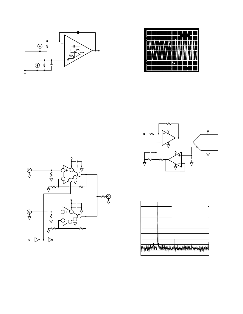
Figure 36. 2:1 Multiplexer
10
0%
1V
200ns
V
S
= +5V
100
90
Figure 37. 2:1 Multiplexer Performance
Single Supply A/D Conversion
Figure 38 shows the AD8041 driving the analog inputs of the
AD9050 in a dc coupled system with single ended signals. All
components are powered from a single +5 V supply. The
AD820 is used to offset the ground referenced input signal to
the level required by the AD9050. The AD8041 is used to add
in the offset with the ground referenced input signal and buffer
the input to AD9050. The nominal input range of the AD9050
0.1μF
+5V
AD8041
2.8V – 3.8V
1000
3.3V
+5V
AD9050
10
9
1000
V
IN
–0.5V TO +0.5V
1000
1000
0.1μF
+5V
AD820
Figure 38. 10-Bit, 40 MSPS A/D Conversion
is +2.8 V and +3.8 V (1 V p-p centered at +3.3 V). This circuit
provides 40 MSPS analog-to-digital conversion on just 330 mW
of power while delivering 10-bit performance.
0
–10
–100
–60
–70
–80
–90
–40
–50
–30
–20
F
= 4.9MHz
FUNDAMENTAL = 0.6dB
2nd HARMONIC = 66.9dB
3rd HARMONIC = 74.7dB
SNR = 55.2dB
NOISE FLOOR = – 86.1dB
ENCODE FREQUENCY = 40MHz
Figure 39. FFT Output of Circuit in Figure 38
相關PDF資料 |
PDF描述 |
|---|---|
| AD8041AN | 160 MHz Rail-to-Rail Amplifier with Disable |
| AD8041AR | 160 MHz Rail-to-Rail Amplifier with Disable |
| AD8041ARZ-REEL | CMOS Low Cost, 10-Bit Multiplying DAC; Package: none available; No of Pins: 16; Temperature Range: Military |
| AD8042ARZ | Dual 160 MHz Rail-to-Rail Amplifier |
| AD8042ARZ-REEL | Dual 160 MHz Rail-to-Rail Amplifier |
相關代理商/技術參數 |
參數描述 |
|---|---|
| AD8041SL-EMX | 制造商:Analog Devices 功能描述:- Bulk |
發布緊急采購,3分鐘左右您將得到回復。