- 您現在的位置:買賣IC網 > PDF目錄373931 > AD8041AN (ANALOG DEVICES INC) 160 MHz Rail-to-Rail Amplifier with Disable PDF資料下載
參數資料
| 型號: | AD8041AN |
| 廠商: | ANALOG DEVICES INC |
| 元件分類: | 運動控制電子 |
| 英文描述: | 160 MHz Rail-to-Rail Amplifier with Disable |
| 中文描述: | OP-AMP, 8000 uV OFFSET-MAX, PDIP8 |
| 封裝: | PLASTIC, DIP-8 |
| 文件頁數: | 14/16頁 |
| 文件大小: | 438K |
| 代理商: | AD8041AN |
REV. 0
–14–
AD8041
To test this, the differential gain and differential phase were
measured for the AD8041 while the supplies were varied. As the
lower supply is raised to approach the video signal, the first ef-
fect to be observed is that the sync tips become compressed be-
fore the differential gain and differential phase are adversely
affected. Thus, there must be adequate swing in the negative di-
rection to pass the sync tips without compression.
As the upper supply is lowered to approach the video, the differ-
ential gain and differential phase were not significantly adversely
affected until the difference between the peak video output and
the supply reached 0.6 V. Thus, the highest video level should
be kept at least 0.6 V below the positive supply rail.
Taking the above into account, it was found that the optimal
point to bias the noninverting input is at 2.2 V dc. Operating at
this point, the worst case differential gain is measured at 0.06%
and the worst case differential phase is 0.06
°
.
The ac coupling capacitors used in the circuit at first glance ap-
pear quite large. A composite video signal has a lower frequency
band edge of 30 Hz. The resistances at the various ac coupling
points—especially at the output—are quite small. In order to
minimize phase shifts and baseline tilt, the large value capacitors
are required. For video system performance that is not to be of
the highest quality, the value of these capacitors can be reduced
by a factor of up to five with only a slightly observable change in
the picture quality.
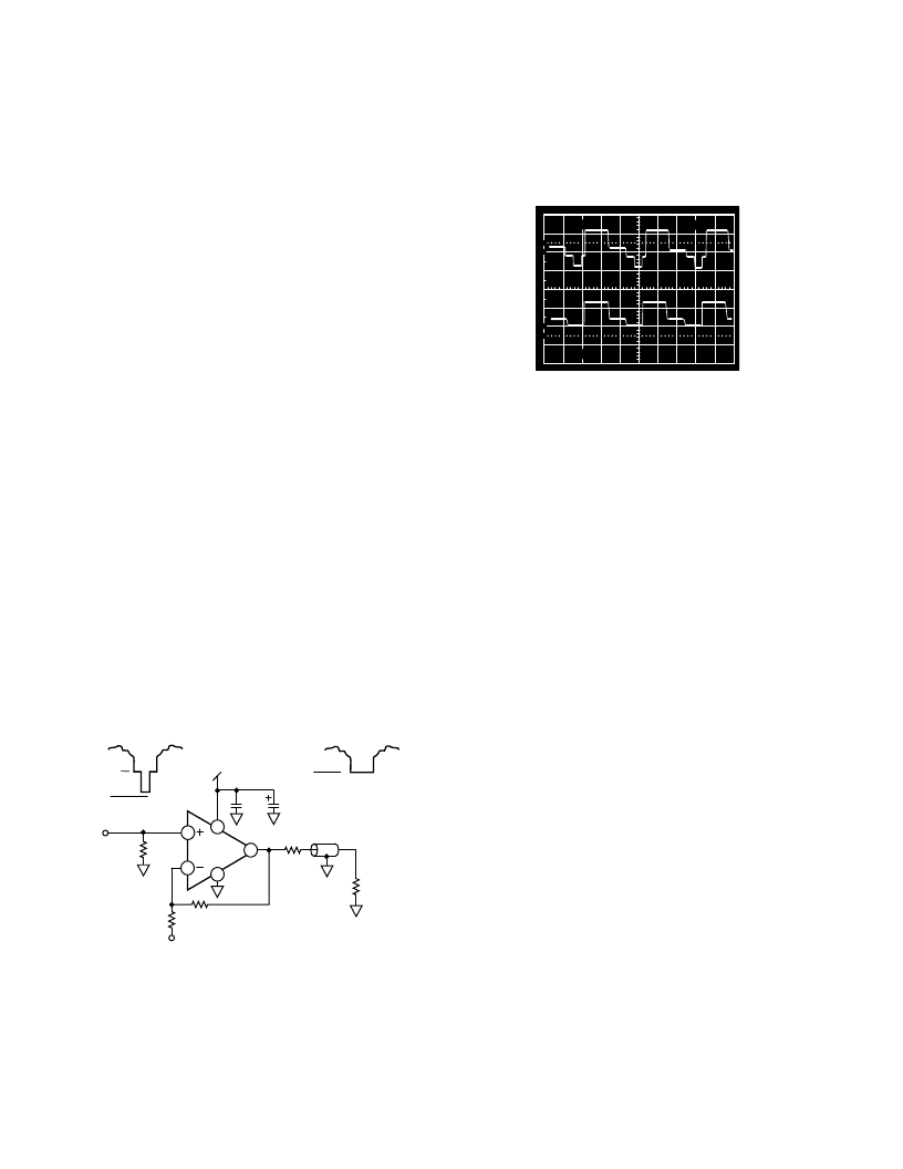
Sync Stripper
Some RGB monitor systems use only three cables total and
carry the synchronizing signals along with the Green (G) signal
on the same cable. The sync signals are pulses that go in the
negative direction from the blanking level of the G signal.
In some applications like prior to digitizing component video
signals with A/D converters, it is desirable to remove or strip the
sync portion from the G signal. Figure 43 is a schematic of a cir-
cuit using the AD8041 running on a single +5 V supply that
performs this function.
AD8041
R2
1k
10μF
0.1μF
0.8V
(2X V
BLANK
)
+5V
75
V
IN
75
75
(MONITOR)
R1
1k
7
6
3
2
4
GREEN W/SYNC
V
BLANK
+0.4
GROUND
GREEN W/OUT SYNC
GROUND
Figure 43. Single Supply Sync Stripper
Referring to Figure 44, the Green plus sync signal is output
from an ADV7120, a single supply triple video DAC. Because
the DAC is single supply, the lowest level of the sync tip is at
ground or slightly above. The AD8041 is set for a gain of two to
compensate for the divide by two of the output terminations.
10
0%
100
90
10μs
500mV
500mV
Figure 44. Single Supply Sync Stripper
The reference voltage for R1 should be twice the dc blanking
level of the G signal. If the blanking level is at ground and the
sync tip is negative as in some dual supply systems, then R1 can
be tied to ground. In either case, the output will have the sync
removed and have the blanking level at ground.
Layout Considerations
The specified high speed performance of the AD8041 requires
careful attention to board layout and component selection.
Proper RF design techniques and low-pass parasitic component
selection are necessary.
The PCB should have a ground plane covering all unused por-
tions of the component side of the board to provide a low im-
pedance path. The ground plane should be removed from the
area near the input pins to reduce the stray capacitance.
Chip capacitors should be used for the supply bypassing (see
Figure 45). One end should be connected to the ground plane
and the other within 1/8 inch of each power pin. An additional
large (0.47
μ
F–10
μ
F) tantalum electrolytic capacitor should be
connected in parallel, but not necessarily so close, to supply cur-
rent for fast, large signal changes at the output.
The feedback resistor should be located close to the inverting
input pin in order to keep the stray capacitance at this node to a
minimum. Capacitance variations of less than 1 pF at the in-
verting input will significantly affect high speed performance.
Stripline design techniques should be used for long signal traces
(greater than about 1 inch). These should be designed with a
characteristic impedance of 50
or 75
and be properly termi-
nated at each end.
相關PDF資料 |
PDF描述 |
|---|---|
| AD8041AR | 160 MHz Rail-to-Rail Amplifier with Disable |
| AD8041ARZ-REEL | CMOS Low Cost, 10-Bit Multiplying DAC; Package: none available; No of Pins: 16; Temperature Range: Military |
| AD8042ARZ | Dual 160 MHz Rail-to-Rail Amplifier |
| AD8042ARZ-REEL | Dual 160 MHz Rail-to-Rail Amplifier |
| AD8042ARZ-REEL7 | Dual 160 MHz Rail-to-Rail Amplifier |
相關代理商/技術參數 |
參數描述 |
|---|---|
| AD8041ANZ | 功能描述:IC OPAMP VF R-R LP LDIST 8DIP RoHS:是 類別:集成電路 (IC) >> Linear - Amplifiers - Instrumentation 系列:- 標準包裝:1 系列:- 放大器類型:通用 電路數:4 輸出類型:滿擺幅 轉換速率:0.028 V/µs 增益帶寬積:105kHz -3db帶寬:- 電流 - 輸入偏壓:3nA 電壓 - 輸入偏移:100µV 電流 - 電源:3.3µA 電流 - 輸出 / 通道:12mA 電壓 - 電源,單路/雙路(±):2.7 V ~ 12 V,±1.35 V ~ 6 V 工作溫度:-40°C ~ 85°C 安裝類型:表面貼裝 封裝/外殼:14-TSSOP(0.173",4.40mm 寬) 供應商設備封裝:14-TSSOP 包裝:剪切帶 (CT) 其它名稱:OP481GRUZ-REELCT |
| AD8041ANZ | 制造商:Analog Devices 功能描述:IC AMP VOLTAGE FEEDBACK |
| AD8041AR | 功能描述:IC OPAMP VF R-R LP LDIST 8SOIC RoHS:否 類別:集成電路 (IC) >> Linear - Amplifiers - Instrumentation 系列:- 標準包裝:73 系列:Over-The-Top® 放大器類型:通用 電路數:4 輸出類型:滿擺幅 轉換速率:0.07 V/µs 增益帶寬積:200kHz -3db帶寬:- 電流 - 輸入偏壓:1nA 電壓 - 輸入偏移:285µV 電流 - 電源:50µA 電流 - 輸出 / 通道:25mA 電壓 - 電源,單路/雙路(±):2 V ~ 44 V,±1 V ~ 22 V 工作溫度:-40°C ~ 85°C 安裝類型:表面貼裝 封裝/外殼:16-WFDFN 裸露焊盤 供應商設備封裝:16-DFN-EP(5x3) 包裝:管件 |
| AD8041AR-EBZ | 功能描述:BOARD EVAL FOR AD8041AR RoHS:是 類別:編程器,開發系統 >> 評估板 - 運算放大器 系列:- 產品培訓模塊:Lead (SnPb) Finish for COTS Obsolescence Mitigation Program 標準包裝:1 系列:- |
| AD8041AR-REEL | 功能描述:IC OPAMP VF R-R LP LDIST 8SOIC RoHS:否 類別:集成電路 (IC) >> Linear - Amplifiers - Instrumentation 系列:- 標準包裝:50 系列:LinCMOS™ 放大器類型:通用 電路數:4 輸出類型:- 轉換速率:0.05 V/µs 增益帶寬積:110kHz -3db帶寬:- 電流 - 輸入偏壓:0.7pA 電壓 - 輸入偏移:210µV 電流 - 電源:57µA 電流 - 輸出 / 通道:30mA 電壓 - 電源,單路/雙路(±):3 V ~ 16 V,±1.5 V ~ 8 V 工作溫度:-40°C ~ 85°C 安裝類型:表面貼裝 封裝/外殼:14-SOIC(0.154",3.90mm 寬) 供應商設備封裝:14-SOIC 包裝:管件 產品目錄頁面:865 (CN2011-ZH PDF) 其它名稱:296-1834296-1834-5 |
發布緊急采購,3分鐘左右您將得到回復。