- 您現在的位置:買賣IC網 > PDF目錄373931 > AD8041ARZ-REEL (ANALOG DEVICES INC) CMOS Low Cost, 10-Bit Multiplying DAC; Package: none available; No of Pins: 16; Temperature Range: Military PDF資料下載
參數資料
| 型號: | AD8041ARZ-REEL |
| 廠商: | ANALOG DEVICES INC |
| 元件分類: | 運動控制電子 |
| 英文描述: | CMOS Low Cost, 10-Bit Multiplying DAC; Package: none available; No of Pins: 16; Temperature Range: Military |
| 中文描述: | OP-AMP, 8000 uV OFFSET-MAX, PDSO8 |
| 封裝: | PLASTIC, LEAD FREE, SOIC-8 |
| 文件頁數: | 11/16頁 |
| 文件大小: | 438K |
| 代理商: | AD8041ARZ-REEL |
AD8041
REV. 0
–11–
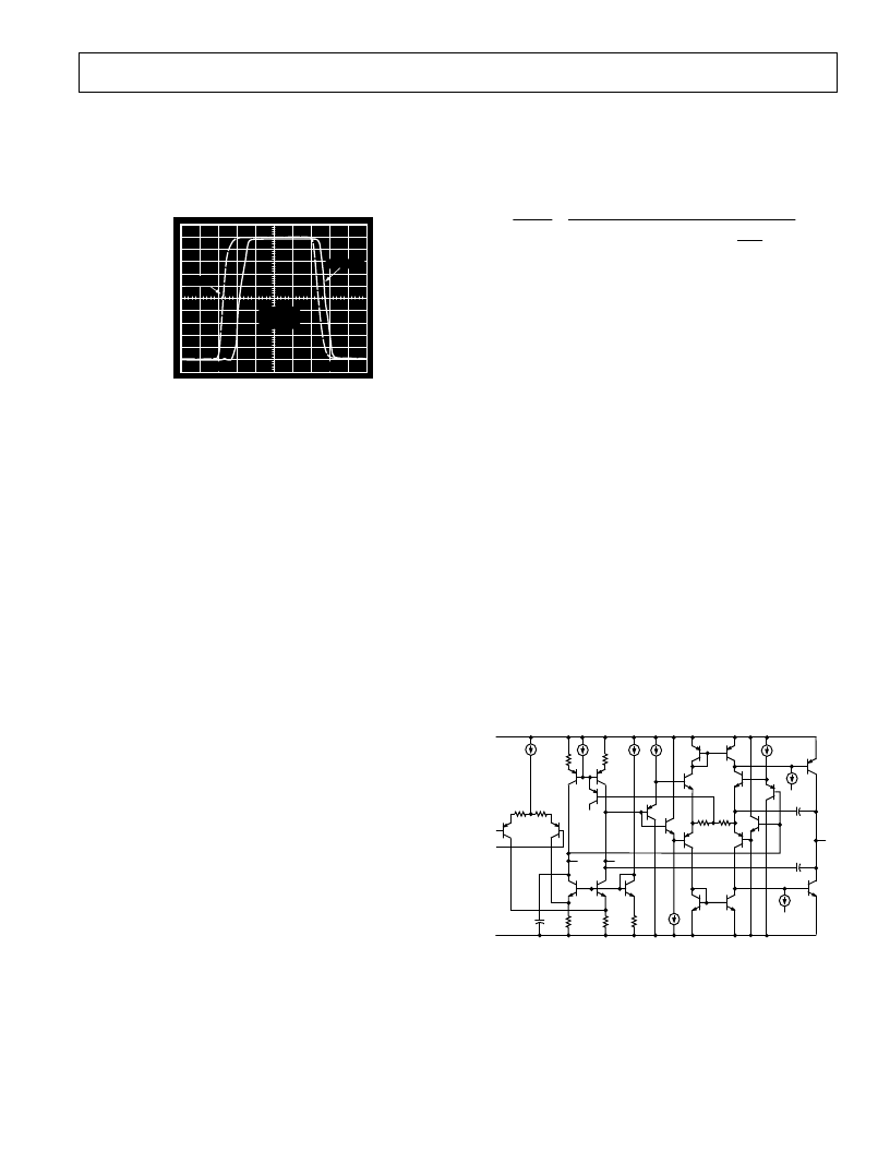
Overdrive Recovery
Overdrive of an amplifier occurs when the output and/or input
range are exceeded. The amplifier must recover from this over-
drive condition. As shown in Figure 33, the AD8041 recovers
within 50 ns from negative overdrive and within 25 ns from
positive overdrive.
5V
2.5V
0V
40ns
50mV
OUTPUT
INPUT
G = +2
V
S
= +5V
Figure 33. Overdrive Recovery
Circuit Description
The AD8041 is fabricated on Analog Devices’ proprietary
eXtra-Fast Complementary Bipolar (XFCB) process which en-
ables the construction of PNP and NPN transistors with similar
f
T
s in the 2 GHz–4 GHz region. The process is dielectrically iso-
lated to eliminate the parasitic and latch-up problems caused by
junction isolation. These features allow the construction of high
frequency, low distortion amplifiers with low supply currents.
This design uses a differential output input stage to maximize
bandwidth and headroom (see Figure 34). The smaller signal
swings required on the first stage outputs (nodes S1P, S1N)
reduce the effect of nonlinear currents due to junction
capacitances and improve the distortion performance. With this
design harmonic distortion of better than –85 dB @ 1 MHz into
100
with V
OUT
= 2 V p-p (Gain = +2) on a single 5 volt sup-
ply is achieved.
The complementary common-emitter design of the output stage
provides excellent load drive without the need for emitter fol-
lowers, thereby improving the output range of the device consid-
erably with respect to conventional op amps. High output drive
capability is provided by injecting all output stage predriver cur-
rents directly into the bases of the output devices Q8 and Q36.
Biasing of Q8 and Q36 is accomplished by I8 and I5, along with
a common-mode feedback loop (not shown). This circuit topol-
ogy allows the AD8041 to drive 50 mA of output current with
the outputs within 0.5 V of the supply rails.
On the input side, the device can handle voltages from –0.2 V
below the negative rail to within 1.2 V of the positive rail. Ex-
ceeding these values will not cause phase reversal; however, the
input ESD devices will begin to conduct if the input voltages ex-
ceed the rails by greater than 0.5 V.
A “Nested Integrator” topology is used in the AD8041 (see
small-signal schematic shown in Figure 35). The output stage
can be modeled as an ideal op amp with a single-pole response
and a unity-gain frequency set by transconductance g
m2
and
capacitor C9. R1 is the output resistance of the input stage; g
m
is the input transconductance. C7 and C9 provide Miller com-
pensation for the overall op amp. The unity gain frequency will
occur at g
m
/C9. Solving the node equations for this circuit
yields:
V
OUT
Vi
=
A0
(sR1[C9(A2
+
1)]
+
1)
×
s
g
m2
C3
+
1
where
A
0 = g
m
g
m2
R2 R1 (Open-Loop Gain of Op Amp)
A
2 = g
m2
R2 (Open-Loop Gain of Output Stage)
The first pole in the denominator is the dominant pole of the
amplifier, and occurs at about 180 Hz. This equals the input
stage output impedance R1 multiplied by the Miller-multiplied
value of C9. The second pole occurs at the unity-gain band-
width of the output stage, which is 250 MHz. This type of
architecture allows more open-loop gain and output drive to be
obtained than a standard two-stage architecture would allow.
Output Impedance
The low frequency open-loop output impedance of the common
emitter output stage used in this design is approximately 6.5 k
.
While this is significantly higher than a typical emitter follower
output stage, when connected with feedback the output imped-
ance is reduced by the open-loop gain of the op amp. With
110 dB of open-loop gain the output impedance is reduced to
less than 0.1
. At higher frequencies the output impedance will
rise as the open-loop gain of the op amp drops; however, the
output also becomes capacitive due to the integrator capacitors
C9 and C3. This prevents the output impedance from ever
becoming excessively high (see Figure 18), which can cause
stability problems when driving capacitive loads. In fact, the
AD8041 has excellent cap-load drive capability for a high-
frequency op amp. Figure 25 demonstrates that the AD8041
exhibits a 45
°
margin while driving a 20 pF direct capacitive
load. In addition, running the part at higher gains will also
improve the capacitive load drive capability of the op amp.
SIN
R21
R3
V
EE
Q11
Q3
I10
R26
R39
Q5
Q4
Q40
I7
R2
R15
Q13
Q17
R5
C7
Q2
SIP
Q22
Q7
Q21
Q24
R23 R27
I2
I3
I1
Q51
Q25
Q50
Q39
Q47
Q27
Q31
Q23
I9
I5
V
EE
V
CC
IB
Q36
Q8
V
OUT
C3
C9
V
CC
V
IN
P
V
IN
N
V
EE
Figure 34. AD8041 Simplified Schematic
相關PDF資料 |
PDF描述 |
|---|---|
| AD8042ARZ | Dual 160 MHz Rail-to-Rail Amplifier |
| AD8042ARZ-REEL | Dual 160 MHz Rail-to-Rail Amplifier |
| AD8042ARZ-REEL7 | Dual 160 MHz Rail-to-Rail Amplifier |
| AD8042 | Dual 160 MHz Rail-to-Rail Amplifier |
| AD8042AN | Dual 160 MHz Rail-to-Rail Amplifier |
相關代理商/技術參數 |
參數描述 |
|---|---|
| AD8041ARZ-REEL1 | 制造商:AD 制造商全稱:Analog Devices 功能描述:160 MHz Rail-to-Rail Amplifier with Disable |
| AD8041ARZ-REEL7 | 功能描述:IC OPAMP VF R-R LP LDIST 8SOIC RoHS:是 類別:集成電路 (IC) >> Linear - Amplifiers - Instrumentation 系列:- 標準包裝:50 系列:LinCMOS™ 放大器類型:通用 電路數:4 輸出類型:- 轉換速率:0.05 V/µs 增益帶寬積:110kHz -3db帶寬:- 電流 - 輸入偏壓:0.7pA 電壓 - 輸入偏移:210µV 電流 - 電源:57µA 電流 - 輸出 / 通道:30mA 電壓 - 電源,單路/雙路(±):3 V ~ 16 V,±1.5 V ~ 8 V 工作溫度:-40°C ~ 85°C 安裝類型:表面貼裝 封裝/外殼:14-SOIC(0.154",3.90mm 寬) 供應商設備封裝:14-SOIC 包裝:管件 產品目錄頁面:865 (CN2011-ZH PDF) 其它名稱:296-1834296-1834-5 |
| AD8041-EB | 制造商:Analog Devices 功能描述: |
| AD8041SL-EMX | 制造商:Analog Devices 功能描述:- Bulk |
發布緊急采購,3分鐘左右您將得到回復。