- 您現在的位置:買賣IC網 > PDF目錄373931 > AD8042 (Analog Devices, Inc.) Dual 160 MHz Rail-to-Rail Amplifier PDF資料下載
參數資料
| 型號: | AD8042 |
| 廠商: | Analog Devices, Inc. |
| 英文描述: | Dual 160 MHz Rail-to-Rail Amplifier |
| 中文描述: | 雙160 MHz的軌到軌放大器 |
| 文件頁數: | 11/15頁 |
| 文件大小: | 181K |
| 代理商: | AD8042 |
AD8042
REV. A
–11–
Overdrive Recovery
Overdrive of an amplifier occurs when the output and/or input
range are exceeded. The amplifier must recover from this over-
drive condition. As shown in Figure 33, the AD8042 recovers
within 30 ns from negative overdrive and within 25 ns from
positive overdrive.
+5V
+2.5V
0V
50ns
1V
V
S
= +5V
V
IN
= +5V p-p
G = +2
R
L
= 1k
V
TO +2.5V
Figure 33. Overdrive Recovery
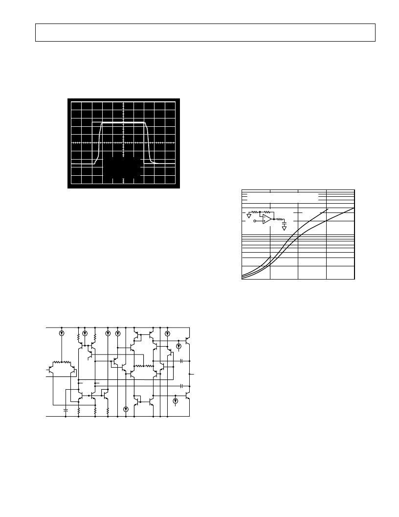
Circuit Description
The AD8042 is fabricated on Analog Devices’ proprietary
eXtra-Fast Complementary Bipolar (XFCB) process which
enables the construction of PNP and NPN transistors with
similar f
T
s in the 2 GHz–4 GHz region. The process is dielectri-
cally isolated to eliminate the parasitic and latch-up problems
caused by junction isolation. These features allow the construc-
tion of high frequency, low distortion amplifiers with low supply
currents. This design uses a differential output input stage to
maximize bandwidth and headroom (see Figure 34). The
smaller signal swings required on the first stage outputs (nodes
S1P, S1N) reduce the effect of nonlinear currents due to
junction capacitances and improve the distortion performance.
With this design harmonic distortion of better than –77 dB
@ 1 MHz into 100
with V
OUT
= 2 V p-p (Gain = +2) on a
single 5 volt supply is achieved.
SIN
R21
R3
V
EE
Q11
Q3
I10
R26
R39
Q5
Q4
Q40
I7
R2
R15
Q13
Q17
R5
C7
Q2
SIP
Q22
Q7
Q21
Q24
R23 R27
I2
I3
I1
Q51
Q25
Q50
Q39
Q47
Q27
Q31
Q23
I9
I5
V
EE
V
CC
I8
Q36
Q8
V
OUT
C3
C9
V
CC
V
IN
P
V
IN
N
V
EE
Figure 34. AD8042 Simplified Schematic
The AD8042’s rail-to-rail output range is provided by a
complementary common-emitter output stage. High output
drive capability is provided by injecting all output stage
predriver currents directly into the bases of the output devices
Q8 and Q36. Biasing of Q8 and Q36 is accomplished by I8 and
I5, along with a common-mode feedback loop (not shown).
This circuit topology allows the AD8042 to drive 40 mA of
output current with the outputs within 0.5V of the supply rails.
On the input side, the device can handle voltages from 0.2 V
below the negative rail to within 1.2 V of the positive rail. Ex-
ceeding these values will not cause phase reversal; however, the
input ESD devices will begin to conduct if the input voltages
exceed the rails by greater than 0.5 V.
DRIVING CAPACITIVE LOADS
The capacitive load drive of the AD8042 can be increased by
adding a low valued resistor in series with the load. Figure 35
shows the effects of a series resistor on capacitive drive for vary-
ing voltage gains. As the closed-loop gain is increased, the larger
phase margin allows for larger capacitive loads with less over-
shoot. Adding a series resistor with lower closed-loop gains
accomplishes this same effect. For large capacitive loads, the
frequency response of the amplifier will be dominated by the
roll-off of the series resistor and capacitive load.
1000
10
100
1
2
5
C
CLOSED-LOOP GAIN – V/V
3
4
R
S
C
L
V
= +5V
200mV STEP WITH 30% OVERSHOOT
R
S
= 20
V
R
S
= 5
V
R
S
= 0
Figure 35. Capacitive Load Drive vs. Closed-Loop Gain
Single Supply Composite Video Line Driver
The two op amps of an AD8042 can be configured as a single
supply dual line driver for composite video. The wide signal
swing of the AD8042 enables this function to be performed
without using any type of clamping or dc restore circuit which
can cause signal distortion.
Figure 36 shows a schematic for a circuit that is driven by a
single composite video source that is ac coupled, level shifted
and applied to both + inputs of the two amplifiers. Each op amp
provides a separate 75
composite video output. To obtain
single supply operation, ac coupling is used throughout. The
large capacitor values are required to ensure that there is mini-
mal tilting of the video signals due to their low frequency
(30 Hz) signal content. The circuit shown was measured to have
a differential gain of 0.06% and a differential phase of 0.06
°
.
The input is terminated in 75
and ac coupled via C
IN
to a
voltage divider that provides the dc bias point to the input.
Setting the optimal bias point requires some understanding of
the nature of composite video signals and the video performance
of the AD8042.
相關PDF資料 |
PDF描述 |
|---|---|
| AD8042AN | Dual 160 MHz Rail-to-Rail Amplifier |
| AD8042AR | Dual 160 MHz Rail-to-Rail Amplifier |
| AD8042AR-REEL | Dual 160 MHz Rail-to-Rail Amplifier |
| AD8042AR-REEL7 | Dual 160 MHz Rail-to-Rail Amplifier |
| AD8042ACHIPS | Dual 160 MHz Rail-to-Rail Amplifier |
相關代理商/技術參數 |
參數描述 |
|---|---|
| AD8042_06 | 制造商:AD 制造商全稱:Analog Devices 功能描述:Dual 160 MHz Rail-to-Rail Amplifier |
| AD8042_07 | 制造商:AD 制造商全稱:Analog Devices 功能描述:Dual 160 MHz Rail-to-Rail Amplifier |
| AD8042ACHIPS | 制造商:Analog Devices 功能描述: |
| AD8042AN | 功能描述:IC OPAMP VF R-R DUAL LP 8DIP RoHS:否 類別:集成電路 (IC) >> Linear - Amplifiers - Instrumentation 系列:- 標準包裝:73 系列:Over-The-Top® 放大器類型:通用 電路數:4 輸出類型:滿擺幅 轉換速率:0.07 V/µs 增益帶寬積:200kHz -3db帶寬:- 電流 - 輸入偏壓:1nA 電壓 - 輸入偏移:285µV 電流 - 電源:50µA 電流 - 輸出 / 通道:25mA 電壓 - 電源,單路/雙路(±):2 V ~ 44 V,±1 V ~ 22 V 工作溫度:-40°C ~ 85°C 安裝類型:表面貼裝 封裝/外殼:16-WFDFN 裸露焊盤 供應商設備封裝:16-DFN-EP(5x3) 包裝:管件 |
| AD8042AR | 功能描述:IC OPAMP VF R-R DUAL LP 8SOIC RoHS:否 類別:集成電路 (IC) >> Linear - Amplifiers - Instrumentation 系列:- 標準包裝:50 系列:- 放大器類型:J-FET 電路數:2 輸出類型:- 轉換速率:13 V/µs 增益帶寬積:3MHz -3db帶寬:- 電流 - 輸入偏壓:65pA 電壓 - 輸入偏移:3000µV 電流 - 電源:1.4mA 電流 - 輸出 / 通道:- 電壓 - 電源,單路/雙路(±):7 V ~ 36 V,±3.5 V ~ 18 V 工作溫度:-40°C ~ 85°C 安裝類型:通孔 封裝/外殼:8-DIP(0.300",7.62mm) 供應商設備封裝:8-PDIP 包裝:管件 |
發布緊急采購,3分鐘左右您將得到回復。