- 您現(xiàn)在的位置:買賣IC網(wǎng) > PDF目錄373934 > AD8061ARZ-REEL (ANALOG DEVICES INC) Low Cost, 300 MHz Rail-to-Rail Amplifiers PDF資料下載
參數(shù)資料
| 型號: | AD8061ARZ-REEL |
| 廠商: | ANALOG DEVICES INC |
| 元件分類: | 運動控制電子 |
| 英文描述: | Low Cost, 300 MHz Rail-to-Rail Amplifiers |
| 中文描述: | OP-AMP, 6000 uV OFFSET-MAX, PDSO8 |
| 封裝: | ROHS COMPLIANT, MS-012AA, SOIC-8 |
| 文件頁數(shù): | 16/20頁 |
| 文件大小: | 302K |
| 代理商: | AD8061ARZ-REEL |
AD8061/AD8062/AD8063
Figure 50 shows a unity-gain follower using the series resistor
strategy. The resistor isolates the output from the capacitance
and, more importantly, creates a zero in the feedback path that
compensates for the pole created by the output capacitance.
Rev. D | Page 16 of 20
VCC
DISABLE
TO AMPLIFIER
BIAS
VEE
2V
0
AD8061
V
O
R
SERIES
C
LOAD
V
IN
0
Figure 52. Disable Circuit of the AD8063
Figure 50. Series Resistor Isolating Capacitive Load
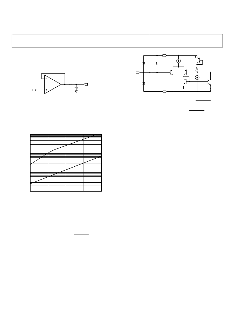
Figure 34 shows the AD8063 supply current vs. DISABLE
voltage. Figure 35 plots the output seen when the AD8063 input
is driven with a 10 MHz sine wave, and the DISABLE is toggled
from 0 V to 5 V, illustrating the part’s turn-on and turn-off
time. Figure 33 shows the input/output isolation response with
the AD8063 shut off.
Voltage feedback amplifiers like those in the AD806x family are
able to drive more capacitive load without excessive peaking
when used in higher gain configurations, because the increased
noise gain reduces the bandwidth of the overall feedback loop.
Figure 51 plots the capacitance that produces 30% overshoot vs.
noise gain for a typical amplifier.
CLOSED-LOOP GAIN
10k
1k
10
1
2
C
100
3
4
5
R
S
= 0
R
S
= 4.7
0
BOARD LAYOUT CONSIDERATIONS
Maintaining the high speed performance of the AD806x family
requires the use of high speed board layout techniques and low
parasitic components.
The PCB should have a ground plane covering unused portions
of the component side of the board to provide a low impedance
path. Remove the ground plane near the package to reduce
parasitic capacitance.
Proper bypassing is critical. Use a ceramic 0.1 μF chip capacitor
to bypass both supplies. Locate the chip capacitor within 3 mm
of each power pin. Additionally, connect in parallel a 4.7 μF to
10 μF tantalum electrolytic capacitor to provide charge for fast,
large signal changes at the output.
Figure 51. Capacitive Load vs. Closed-Loop Gain
Minimizing parasitic capacitance at the amplifier’s inverting
input pin is very important. Locate the feedback resistor close to
the inverting input pin. The value of the feedback resistor may
come into play—for instance, 1 kΩ interacting with 1 pF of
parasitic capacitance creates a pole at 159 MHz. Use stripline
design techniques for signal traces longer than 25 mm. Design
them with either 50 Ω or 75 Ω characteristic impedance and
proper termination at each end.
DISABLE OPERATION
The internal circuit for the AD8063 disable function is shown
in Figure 52. When the DISABLE node is pulled below 2 V
from the positive supply, the supply current decreases from
typically 6.5 mA to under 400 μA, and the AD8063 output
will enter a high impedance state. If the DISABLE node is not
connected and allowed to float, the AD8063 stays biased at
full power.
相關(guān)PDF資料 |
PDF描述 |
|---|---|
| AD8061ARZ-REEL7 | Low Cost, 300 MHz Rail-to-Rail Amplifiers |
| AD8062ARMZ | Low Cost, 300 MHz Rail-to-Rail Amplifiers |
| AD8062ARMZ-R7 | Low Cost, 300 MHz Rail-to-Rail Amplifiers |
| AD8062ARZ-RL | Low Cost, 300 MHz Rail-to-Rail Amplifiers |
| AD8063ART-R2 | Low Cost, 300 MHz Rail-to-Rail Amplifiers |
相關(guān)代理商/技術(shù)參數(shù) |
參數(shù)描述 |
|---|---|
| AD8061ARZREEL7 | 制造商:Analog Devices 功能描述: |
| AD8061ARZ-REEL7 | 功能描述:IC OPAMP VF R-R LP 50MA 8SOIC RoHS:是 類別:集成電路 (IC) >> Linear - Amplifiers - Instrumentation 系列:- 標(biāo)準(zhǔn)包裝:160 系列:- 放大器類型:通用 電路數(shù):4 輸出類型:滿擺幅 轉(zhuǎn)換速率:10 V/µs 增益帶寬積:9MHz -3db帶寬:- 電流 - 輸入偏壓:1pA 電壓 - 輸入偏移:250µV 電流 - 電源:730µA 電流 - 輸出 / 通道:28mA 電壓 - 電源,單路/雙路(±):2.7 V ~ 5.5 V,±1.35 V ~ 2.75 V 工作溫度:-40°C ~ 125°C 安裝類型:表面貼裝 封裝/外殼:16-SOIC(0.154",3.90mm 寬) 供應(yīng)商設(shè)備封裝:16-SOIC N 包裝:管件 |
| AD8062AR | 功能描述:IC OPAMP VF R-R DUAL LP 8SOIC RoHS:否 類別:集成電路 (IC) >> Linear - Amplifiers - Instrumentation 系列:- 標(biāo)準(zhǔn)包裝:50 系列:- 放大器類型:J-FET 電路數(shù):2 輸出類型:- 轉(zhuǎn)換速率:3.5 V/µs 增益帶寬積:1MHz -3db帶寬:- 電流 - 輸入偏壓:30pA 電壓 - 輸入偏移:2000µV 電流 - 電源:200µA 電流 - 輸出 / 通道:- 電壓 - 電源,單路/雙路(±):7 V ~ 36 V,±3.5 V ~ 18 V 工作溫度:0°C ~ 70°C 安裝類型:通孔 封裝/外殼:8-DIP(0.300",7.62mm) 供應(yīng)商設(shè)備封裝:8-PDIP 包裝:管件 |
| AD8062AR-EBZ | 功能描述:BOARD EVAL FOR AD8062AR RoHS:是 類別:編程器,開發(fā)系統(tǒng) >> 評估板 - 運算放大器 系列:- 產(chǎn)品培訓(xùn)模塊:Lead (SnPb) Finish for COTS Obsolescence Mitigation Program 標(biāo)準(zhǔn)包裝:1 系列:- |
| AD8062ARM | 功能描述:IC OPAMP VF R-R DUAL LP 8MSOP RoHS:否 類別:集成電路 (IC) >> Linear - Amplifiers - Instrumentation 系列:- 標(biāo)準(zhǔn)包裝:50 系列:- 放大器類型:J-FET 電路數(shù):2 輸出類型:- 轉(zhuǎn)換速率:3.5 V/µs 增益帶寬積:1MHz -3db帶寬:- 電流 - 輸入偏壓:30pA 電壓 - 輸入偏移:2000µV 電流 - 電源:200µA 電流 - 輸出 / 通道:- 電壓 - 電源,單路/雙路(±):7 V ~ 36 V,±3.5 V ~ 18 V 工作溫度:0°C ~ 70°C 安裝類型:通孔 封裝/外殼:8-DIP(0.300",7.62mm) 供應(yīng)商設(shè)備封裝:8-PDIP 包裝:管件 |
發(fā)布緊急采購,3分鐘左右您將得到回復(fù)。