- 您現(xiàn)在的位置:買賣IC網(wǎng) > PDF目錄373934 > AD8062ARMZ (ANALOG DEVICES INC) Low Cost, 300 MHz Rail-to-Rail Amplifiers PDF資料下載
參數(shù)資料
| 型號(hào): | AD8062ARMZ |
| 廠商: | ANALOG DEVICES INC |
| 元件分類: | 運(yùn)動(dòng)控制電子 |
| 英文描述: | Low Cost, 300 MHz Rail-to-Rail Amplifiers |
| 中文描述: | DUAL OP-AMP, 6000 uV OFFSET-MAX, PDSO8 |
| 封裝: | ROHS COMPLIANT, MO-187AA, MSOP-8 |
| 文件頁數(shù): | 15/20頁 |
| 文件大小: | 302K |
| 代理商: | AD8062ARMZ |
AD8061/AD8062/AD8063
Rev. D | Page 15 of 20
TIME (ns)
2.0
0
O
2.2
2.4
2.6
2.8
3.0
3.2
3.4
3.6
4
8
12
16
20
24
28
32
2V TO 3V STEP
2.1V TO 3.1V STEP
2.2V TO 3.2V STEP
2.3V TO 3.3V STEP
2.4V TO 3.4V STEP
0
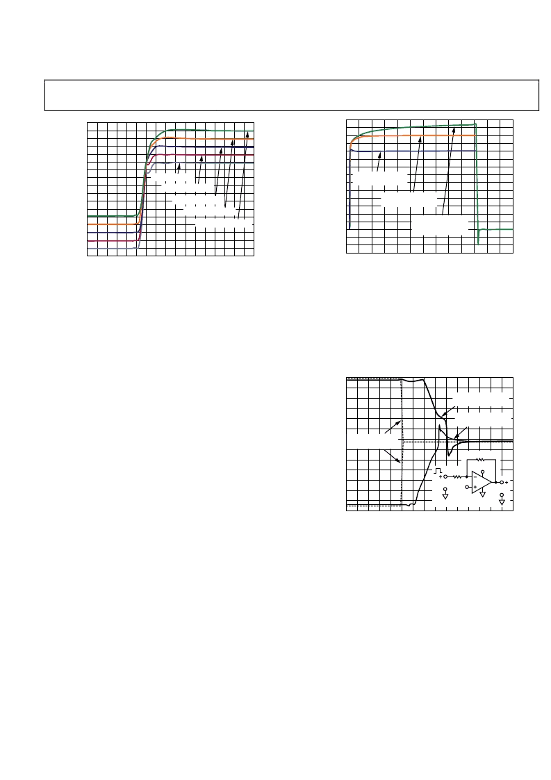
Figure 47. Output Rising Edge for 1 V Step at
Input Headroom Limits, G = 1, V
S
= 5 V, 0 V
As the saturation point of the output stage is approached, the
output signal shows increasing amounts of compression and
clipping. As in the input headroom case, the higher frequency
signals require a bit more headroom than lower frequency
signals. Figure 16, Figure 17, and Figure 18 illustrate this point,
plotting typical distortion vs. output amplitude and bias for
gains of 2 and 5.
OVERLOAD BEHAVIOR AND RECOVERY
Input
The specified input common-mode voltage of the AD806x
is 200 mV below the negative supply to within 1.8 V of
the positive supply. Exceeding the top limit results in lower
bandwidth and increased settling time as seen in Figure 46
and Figure 47. Pushing the input voltage of a unity-gain
follower beyond 1.6 V within the positive supply leads to the
behavior shown in Figure 48—an increasing amount of output
error and much increased settling time. Recovery time from
input voltages 1.6 V or closer to the positive supply is approxi-
mately 35 ns, which is limited by the settling artifacts caused by
transistors in the input stage coming out of saturation.
The AD806x family does not exhibit phase reversal, even for
input voltages beyond the voltage supply rails. Going more
than 0.6 V beyond the power supplies will turn on protection
diodes at the input stage, which will greatly increase the device’s
current draw.
TIME (ns)
2.1
0
O
2.3
100
VOLTAGE STEP
FROM 2.4V TO 3.4V
2.5
2.7
2.9
3.1
3.3
3.5
3.7
VOLTAGE STEP
FROM 2.4V TO 3.6V
VOLTAGE STEP
FROM 2.4V TO 3.8V,
4V AND 5V
200
300
400
500
600
0
Figure 48. Pulse Response for G = 1 Follower,
Input Step Overloading the Input Stage
Output
Output overload recovery is typically within 40 ns after the
amplifier’s input is brought to a nonoverloading value. Figure 49
shows output recovery transients for the amplifier recovering
from a saturated output from the top and bottom supplies to a
point at midsupply.
TIME (ns)
–
0.2
I
OUTPUT VOLTAGE
5V TO 2.5V
0.2
0.6
1.0
1.4
1.8
2.2
2.6
3.0
3.4
3.8
4.2
4.6
5.0
10
20
30
40
50
60
70
OUTPUT VOLTAGE
0V TO 2.5V
INPUT VOLTAGE
EDGES
R
5V
V
O
2.5V
R
V
IN
–
–
0
0
Figure 49. Overload Recovery, G = 1, V
S
= 5 V
CAPACITIVE LOAD DRIVE
The AD806x family is optimized for bandwidth and speed, not
for driving capacitive loads. Output capacitance creates a pole
in the amplifier’s feedback path, leading to excessive peaking
and potential oscillation. If dealing with load capacitance is a
requirement of the application, the two strategies to consider
are as follows:
1.
Use a small resistor in series with the amplifier’s output and
the load capacitance.
2.
Reduce the bandwidth of the amplifier’s feedback loop by
increasing the overall noise gain.
相關(guān)PDF資料 |
PDF描述 |
|---|---|
| AD8062ARMZ-R7 | Low Cost, 300 MHz Rail-to-Rail Amplifiers |
| AD8062ARZ-RL | Low Cost, 300 MHz Rail-to-Rail Amplifiers |
| AD8063ART-R2 | Low Cost, 300 MHz Rail-to-Rail Amplifiers |
| AD8063ARTZ-R2 | Low Cost, 300 MHz Rail-to-Rail Amplifiers |
| AD8063ARTZ-REEL | Low Cost, 300 MHz Rail-to-Rail Amplifiers |
相關(guān)代理商/技術(shù)參數(shù) |
參數(shù)描述 |
|---|---|
| AD8062ARMZ-R7 | 功能描述:IC OPAMP VF R-R DUAL LP 8MSOP RoHS:是 類別:集成電路 (IC) >> Linear - Amplifiers - Instrumentation 系列:- 產(chǎn)品培訓(xùn)模塊:Differential Circuit Design Techniques for Communication Applications 標(biāo)準(zhǔn)包裝:1 系列:- 放大器類型:RF/IF 差分 電路數(shù):1 輸出類型:差分 轉(zhuǎn)換速率:9800 V/µs 增益帶寬積:- -3db帶寬:2.9GHz 電流 - 輸入偏壓:3µA 電壓 - 輸入偏移:- 電流 - 電源:40mA 電流 - 輸出 / 通道:- 電壓 - 電源,單路/雙路(±):3 V ~ 3.6 V 工作溫度:-40°C ~ 85°C 安裝類型:表面貼裝 封裝/外殼:16-VQFN 裸露焊盤,CSP 供應(yīng)商設(shè)備封裝:16-LFCSP-VQ 包裝:剪切帶 (CT) 產(chǎn)品目錄頁面:551 (CN2011-ZH PDF) 其它名稱:ADL5561ACPZ-R7CT |
| AD8062ARMZ-RL | 功能描述:IC OPAMP VF R-R DUAL LP 8MSOP RoHS:是 類別:集成電路 (IC) >> Linear - Amplifiers - Instrumentation 系列:- 標(biāo)準(zhǔn)包裝:50 系列:- 放大器類型:通用 電路數(shù):2 輸出類型:滿擺幅 轉(zhuǎn)換速率:1.8 V/µs 增益帶寬積:6.5MHz -3db帶寬:4.5MHz 電流 - 輸入偏壓:5nA 電壓 - 輸入偏移:100µV 電流 - 電源:65µA 電流 - 輸出 / 通道:35mA 電壓 - 電源,單路/雙路(±):1.8 V ~ 5.25 V,±0.9 V ~ 2.625 V 工作溫度:-40°C ~ 85°C 安裝類型:表面貼裝 封裝/外殼:10-TFSOP,10-MSOP(0.118",3.00mm 寬) 供應(yīng)商設(shè)備封裝:10-MSOP 包裝:管件 |
| AD8062AR-REEL | 制造商:Analog Devices 功能描述:OP Amp Dual Volt Fdbk R-R O/P 8V 8-Pin SOIC N T/R 制造商:Rochester Electronics LLC 功能描述:SOIC DUAL, RAIL-TO-RAIL VLTG-FDBK AMP - Tape and Reel |
| AD8062AR-REEL7 | 制造商:Analog Devices 功能描述:OP Amp Dual Volt Fdbk R-R O/P 8V 8-Pin SOIC N T/R 制造商:Rochester Electronics LLC 功能描述:SOIC DUAL, RAIL-TO-RAIL VLTG-FDBK AMP - Tape and Reel |
| AD8062ARZ | 功能描述:IC OPAMP VF R-R DUAL LP 8SOIC RoHS:是 類別:集成電路 (IC) >> Linear - Amplifiers - Instrumentation 系列:- 產(chǎn)品培訓(xùn)模塊:Differential Circuit Design Techniques for Communication Applications 標(biāo)準(zhǔn)包裝:1 系列:- 放大器類型:RF/IF 差分 電路數(shù):1 輸出類型:差分 轉(zhuǎn)換速率:9800 V/µs 增益帶寬積:- -3db帶寬:2.9GHz 電流 - 輸入偏壓:3µA 電壓 - 輸入偏移:- 電流 - 電源:40mA 電流 - 輸出 / 通道:- 電壓 - 電源,單路/雙路(±):3 V ~ 3.6 V 工作溫度:-40°C ~ 85°C 安裝類型:表面貼裝 封裝/外殼:16-VQFN 裸露焊盤,CSP 供應(yīng)商設(shè)備封裝:16-LFCSP-VQ 包裝:剪切帶 (CT) 產(chǎn)品目錄頁面:551 (CN2011-ZH PDF) 其它名稱:ADL5561ACPZ-R7CT |
發(fā)布緊急采購(gòu),3分鐘左右您將得到回復(fù)。