- 您現在的位置:買賣IC網 > PDF目錄373934 > AD8063ARZ-REEL (ANALOG DEVICES INC) Low Cost, 300 MHz Rail-to-Rail Amplifiers PDF資料下載
參數資料
| 型號: | AD8063ARZ-REEL |
| 廠商: | ANALOG DEVICES INC |
| 元件分類: | 運動控制電子 |
| 英文描述: | Low Cost, 300 MHz Rail-to-Rail Amplifiers |
| 中文描述: | OP-AMP, 6000 uV OFFSET-MAX, PDSO8 |
| 封裝: | LEAD FREE, MS-012AA, SOIC-8 |
| 文件頁數: | 14/20頁 |
| 文件大小: | 302K |
| 代理商: | AD8063ARZ-REEL |
AD8061/AD8062/AD8063
CIRCUIT DESCRIPTION
The AD8061/AD8062/AD8063 family is comprised of high
speed voltage feedback op amps. The high slew rate input stage
is a true, single-supply topology, capable of sensing signals at or
below the minus supply rail. The rail-to-rail output stage can
pull within 30 mV of either supply rail when driving light loads
and within 0.3 V when driving 150 Ω. High speed perform-
ance is maintained at supply voltages as low as 2.7 V.
Rev. D | Page 14 of 20
HEADROOM CONSIDERATIONS
These amplifiers are designed for use in low voltage systems.
To obtain optimum performance, it is useful to understand the
behavior of the amplifier as input and output signals approach
the amplifier’s headroom limits.
The AD806x’s input common-mode voltage range extends
from the negative supply voltage (actually 200 mV below this),
or ground for single-supply operation, to within 1.8 V of the
positive supply voltage. Thus, at a gain of 2, the AD806x can
provide full rail-to-rail output swing for supply voltage as low as
3.6 V, assuming the input signal swing from V
S
(or ground) to
+V
S
/2. At a gain of 3, the AD806x can provide a rail-to-rail
output range down to 2.7 V total supply voltage.
Exceeding the headroom limit is not a concern for any inverting
gain on any supply voltage, as long as the reference voltage at
the amplifier’s positive input lies within the amplifier’s input
common-mode range.
The input stage is the headroom limit for signals when the
amplifier is used in a gain of 1 for signals approaching the
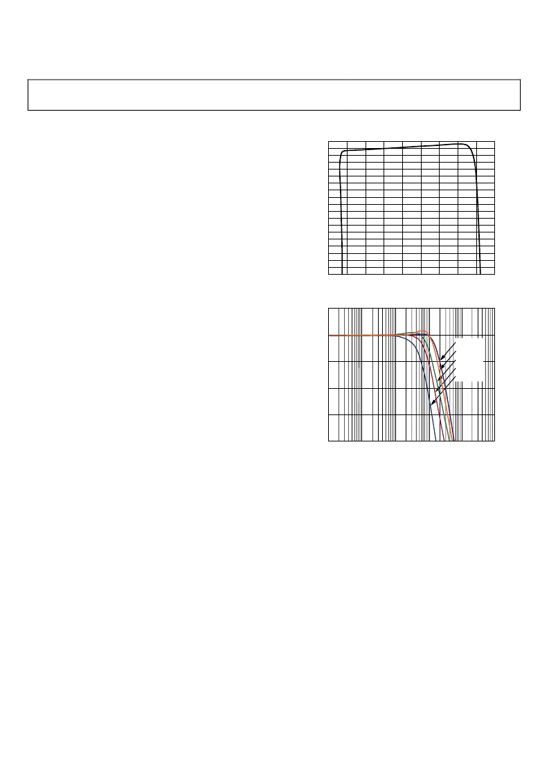
positive rail. Figure 45 shows a typical offset voltage vs.
input common-mode voltage for the AD806x amplifier on
a 5 V supply. Accurate dc performance is maintained from
approximately 200 mV below the minus supply to within
1.8 V of the positive supply. For high-speed signals, however,
there are other considerations. Figure 46 shows 3 dB
bandwidth vs. dc input voltage for a unity-gain follower. As
the common-mode voltage approaches the positive supply,
the amplifier holds together well, but the bandwidth begins to
drop at 1.9 V within +V
S
.
This manifests itself in increased distortion or settling time.
Figure 16 plots the distortion of a 1 V p-p signal with the
AD806x amplifier used as a follower on a 5 V supply vs. signal
common-mode voltage. Distortion performance is maintained
until the input signal center voltage gets beyond 2.5 V, as the
peak of the input sine wave begins to run into the upper
common-mode voltage limit.
V
CM
(V)
V
O
–4.0
–3.6
–3.2
–2.8
–2.4
–2.0
–1.6
–1.2
–0.8
–0.4
–0.5
0
0.5
1.0
1.5
2.0
2.5
3.0
3.5
4.0
0
Figure 45. V
OS
vs. Common-Mode Voltage, V
S
= 5 V
V
CM
= 3.0
V
CM
= 3.1
V
CM
= 3.2
V
CM
= 3.3
V
CM
= 3.4
FREQUENCY (MHz)
2
–8
0.1
G
–4
0
–2
–6
1
10
100
1k
10k
0
Figure 46. Unity-Gain Follower Bandwidth vs. Input Common Mode, V
S
= 5 V
Higher frequency signals require more headroom than lower
frequencies to maintain distortion performance. Figure 47
illustrates how the rising edge settling time for the amplifier
configured as a unity-gain follower stretches out as the top of
a 1 V step input approaches and exceeds the specified input
common-mode voltage limit.
For signals approaching the minus supply and inverting gain
and high positive gain configurations, the headroom limit is
the output stage. The AD806x amplifiers use a common emitter
style output stage. This output stage maximizes the available
output range, limited by the saturation voltage of the output
transistors. The saturation voltage increases with the drive
current the output transistor is required to supply, due to the
output transistors’ collector resistance. The saturation voltage is
estimated using the equation
V
SAT
= 25 mV +
I
O
×
8 Ω, where
I
O
is the output current, and 8 Ω is a typical value for the output
transistors’ collector resistance.
相關PDF資料 |
PDF描述 |
|---|---|
| AD8063ARZ-REEL7 | Low Cost, 300 MHz Rail-to-Rail Amplifiers |
| AD8062ARMZ-RL | Low Cost, 300 MHz Rail-to-Rail Amplifiers |
| AD8062ARZ1 | Low Cost, 300 MHz Rail-to-Rail Amplifiers |
| AD8062ARZ-R7 | Low Cost, 300 MHz Rail-to-Rail Amplifiers |
| AD8064 | Low Cost, 275MHz Rail-to Rail Amplifiers(低成本,滿幅度四放大器) |
相關代理商/技術參數 |
參數描述 |
|---|---|
| AD8063ARZ-REEL7 | 功能描述:IC OPAMP VF R-R LP 50MA 8SOIC RoHS:是 類別:集成電路 (IC) >> Linear - Amplifiers - Instrumentation 系列:- 標準包裝:160 系列:- 放大器類型:通用 電路數:4 輸出類型:滿擺幅 轉換速率:10 V/µs 增益帶寬積:9MHz -3db帶寬:- 電流 - 輸入偏壓:1pA 電壓 - 輸入偏移:250µV 電流 - 電源:730µA 電流 - 輸出 / 通道:28mA 電壓 - 電源,單路/雙路(±):2.7 V ~ 5.5 V,±1.35 V ~ 2.75 V 工作溫度:-40°C ~ 125°C 安裝類型:表面貼裝 封裝/外殼:16-SOIC(0.154",3.90mm 寬) 供應商設備封裝:16-SOIC N 包裝:管件 |
| AD8065AR | 功能描述:IC OPAMP VF R-R LN LP 30MA 8SOIC RoHS:否 類別:集成電路 (IC) >> Linear - Amplifiers - Instrumentation 系列:FastFET™ 標準包裝:1 系列:- 放大器類型:通用 電路數:4 輸出類型:滿擺幅 轉換速率:0.028 V/µs 增益帶寬積:105kHz -3db帶寬:- 電流 - 輸入偏壓:3nA 電壓 - 輸入偏移:100µV 電流 - 電源:3.3µA 電流 - 輸出 / 通道:12mA 電壓 - 電源,單路/雙路(±):2.7 V ~ 12 V,±1.35 V ~ 6 V 工作溫度:-40°C ~ 85°C 安裝類型:表面貼裝 封裝/外殼:14-TSSOP(0.173",4.40mm 寬) 供應商設備封裝:14-TSSOP 包裝:剪切帶 (CT) 其它名稱:OP481GRUZ-REELCT |
| AD8065AR-EBZ | 功能描述:BOARD EVAL FOR AD8065AR RoHS:是 類別:編程器,開發系統 >> 評估板 - 運算放大器 系列:- 產品培訓模塊:Lead (SnPb) Finish for COTS Obsolescence Mitigation Program 標準包裝:1 系列:- |
| AD8065AR-REEL | 制造商:Analog Devices 功能描述:OP Amp Single Volt Fdbk R-R O/P 制造商:Analog Devices 功能描述:OP Amp Single Volt Fdbk R-R O/P ±12V/24V 8-Pin SOIC N T/R |
| AD8065AR-REEL7 | 制造商:Analog Devices 功能描述:OP Amp Single Volt Fdbk R-R O/P 制造商:Analog Devices 功能描述:OP Amp Single Volt Fdbk R-R O/P ±12V/24V 8-Pin SOIC N T/R 制造商:Rochester Electronics LLC 功能描述:SOIC HI PERF HI SPD FET AMP W/ DISABLE - Tape and Reel |
發布緊急采購,3分鐘左右您將得到回復。