- 您現在的位置:買賣IC網 > PDF目錄373937 > AD8130ARM-REEL3 (Analog Devices, Inc.) Low-Cost 270 MHz Differential Receiver Amplifiers PDF資料下載
參數資料
| 型號: | AD8130ARM-REEL3 |
| 廠商: | Analog Devices, Inc. |
| 英文描述: | Low-Cost 270 MHz Differential Receiver Amplifiers |
| 中文描述: | 低成本270 MHz的差分接收器放大器 |
| 文件頁數: | 24/28頁 |
| 文件大小: | 510K |
| 代理商: | AD8130ARM-REEL3 |
第1頁第2頁第3頁第4頁第5頁第6頁第7頁第8頁第9頁第10頁第11頁第12頁第13頁第14頁第15頁第16頁第17頁第18頁第19頁第20頁第21頁第22頁第23頁當前第24頁第25頁第26頁第27頁第28頁
REV. 0
AD8129/AD8130
–24–
The center conductor connects to the positive differential input
of the AD8130. The amplitude of the video signal at this point
is unity, because it is between the two termination resistors. The
AD8130 provides a high impedance to this signal, so it does not
disturb it. A buffered, unity-gain version of the video signal
appears at the output.
Power-Down
The AD8129/AD8130 have a power-down pin that can be used
to lower the quiescent current when the amplifier is not being
used. A logic low level on the PD pin will cause the part to
power down.
Since there is no “Ground” pin on the AD8129/AD8130, there
is no logic reference to interface to standard logic levels. For
this reason, the reference level for the
PD
input is +V
S
. If the
AD8129/AD8130 are run with +V
S
= 5 V, there will be direct
compatibility with logic families. However, if +V
S
is higher
than this, a level-shift circuit will be needed to interface to con-
ventional logic levels. A simple level-shifting circuit that is
compatible with common logic families is presented in Figure 17.
AD8129/
AD8130
7
+V
S
+V
S
3
PD
1k
4.99k
LOW=
POWER-DOWN
2N2222
OR EQ
Figure 17. Circuit that Shifts the Logic Level when +V
S
Is
Not Equal to Approximately 5 V
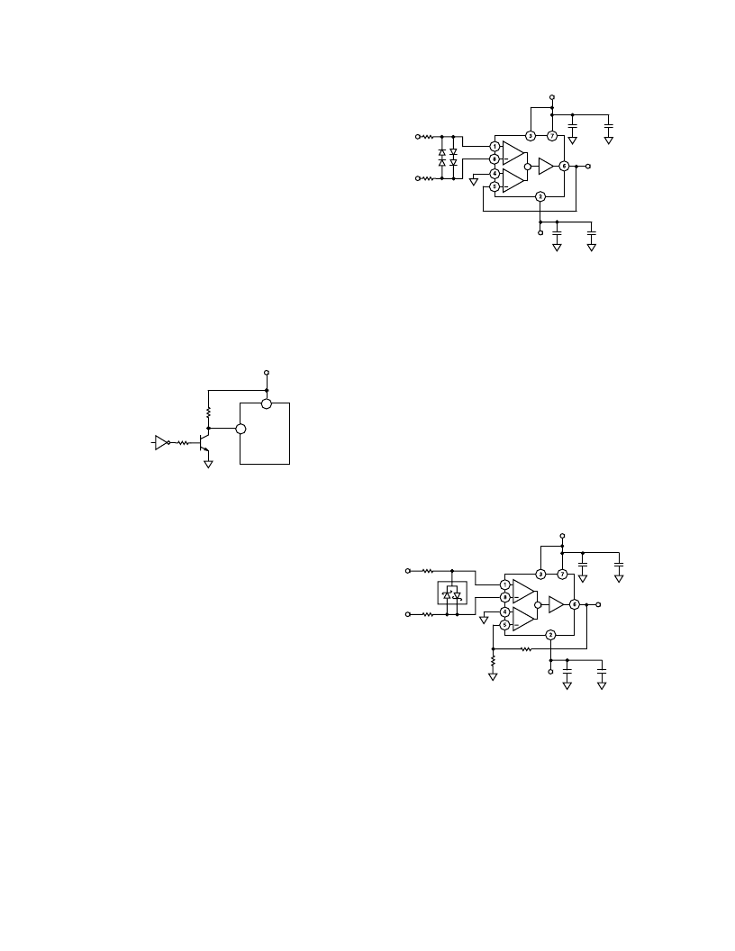
Extreme Operating Conditions
The AD8129/AD8130 are designed to provide high perfor-
mance over a wide range of supply voltages. However, there are
some extremes of operating conditions that have been observed
to produce non-optimal results. One of these conditions occurs
when the AD8130 is operated at unity gain with low supply
voltage—less than approximately
±
4 V.
At unity gain, the output drives FB directly. At supplies of
±
V
S
less than approximately
±
4 V and unity gain, the voltage on FB
can be driven by the output too close to the rail for the circuit to
stay properly biased. This can lead to a parasitic oscillation.
A way to prevent this is to limit the input signal swing with
clamp diodes. Common silicon junction signal diodes like the
1N4148 have a forward bias of approximately 0.7 V when about
1 mA of current flow through them. Two series pairs of such
diodes connected antiparallel across the differential inputs can
be used to clamp the input signal and prevent this condition. It
should be noted that the REF input can also shift the output
signal, so this technique will only work when REF is at ground
or close to it. (See Figure 18.)
AD8130
V
OUT
0.1 F
10 F
–
V
+V
0.1 F
10 F
–
V
S
PD
+V
S
+
+
V
IN
1N4148
V
IN
Figure 18. Clamping Diodes at the Input Limit the Input
Swing Amplitude
Another problem can occur with the AD8129 operating at supply
voltage of greater than or equal to
±
12 V. The architecture
causes the supply current to increase as the input differential
voltage increases. If the AD8129 differential inputs are over-
driven too far, excessive current can flow in the device and
potentially cause permanent damage.
A practical means to prevent this from occurring is to differentially
clamp the inputs with a pair of antiparallel Schottky diodes.
(See Figure 19.) These diodes have a lower forward voltage
of approximately 0.4 V. If the differential voltage across the
inputs is restricted to these conditions, no excess current will
be drawn by the AD8129 under these operating conditions.
If the supply voltage is restricted to less than
±
11 V, the internal
clamping circuit will limit the differential voltage and excessive
supply current will not be drawn. The external clamp circuit is
not needed.
V
IN
AGILENT
HSMS 2822
1
2
3
V
OUT
0.1 F
10 F
–
V
+V
0.1 F
10 F
–
V
S
PD
+V
S
+
+
V
IN
AD8129
Figure 19. Schottky Diodes Across the Inputs Limits the
Input Differential Voltage
In both circuits, the input series resistors function to limit the
current through the diodes when they are forward-biased. As a
practical matter, these resistors need to be matched to the degree
that the CMRR needs to be preserved at high frequency. These
resistor will have minimal effect on the CMRR at low frequency.
相關PDF資料 |
PDF描述 |
|---|---|
| AD8130ARM-REEL72 | Low-Cost 270 MHz Differential Receiver Amplifiers |
| AD8129 | Low-Cost 270 MHz Differential Receiver Amplifiers |
| AD8129-EVAL | Low-Cost 270 MHz Differential Receiver Amplifiers |
| AD8129AR-REEL1 | Low-Cost 270 MHz Differential Receiver Amplifiers |
| AD8129AR-REEL72 | Low-Cost 270 MHz Differential Receiver Amplifiers |
相關代理商/技術參數 |
參數描述 |
|---|---|
| AD8130ARM-REEL7 | 制造商:Analog Devices 功能描述:SP Amp DIFF Receiver Amp Single 制造商:Analog Devices 功能描述:SP Amp DIFF Receiver Amp Single ±12.6V/25.2V 8-Pin MSOP T/R |
| AD8130ARM-REEL72 | 制造商:AD 制造商全稱:Analog Devices 功能描述:Low-Cost 270 MHz Differential Receiver Amplifiers |
| AD8130ARMZ | 功能描述:IC AMP DIFF LN LDIST 40MA 8MSOP RoHS:是 類別:集成電路 (IC) >> Linear - Amplifiers - Instrumentation 系列:- 產品培訓模塊:Differential Circuit Design Techniques for Communication Applications 標準包裝:1 系列:- 放大器類型:RF/IF 差分 電路數:1 輸出類型:差分 轉換速率:9800 V/µs 增益帶寬積:- -3db帶寬:2.9GHz 電流 - 輸入偏壓:3µA 電壓 - 輸入偏移:- 電流 - 電源:40mA 電流 - 輸出 / 通道:- 電壓 - 電源,單路/雙路(±):3 V ~ 3.6 V 工作溫度:-40°C ~ 85°C 安裝類型:表面貼裝 封裝/外殼:16-VQFN 裸露焊盤,CSP 供應商設備封裝:16-LFCSP-VQ 包裝:剪切帶 (CT) 產品目錄頁面:551 (CN2011-ZH PDF) 其它名稱:ADL5561ACPZ-R7CT |
| AD8130ARMZ | 制造商:Analog Devices 功能描述:Operational Amplifier (Op-Amp) IC |
| AD8130ARMZ-REEL | 功能描述:IC AMP DIFF LN LDIST 40MA 8MSOP RoHS:是 類別:集成電路 (IC) >> Linear - Amplifiers - Instrumentation 系列:- 標準包裝:50 系列:- 放大器類型:通用 電路數:2 輸出類型:滿擺幅 轉換速率:1.8 V/µs 增益帶寬積:6.5MHz -3db帶寬:4.5MHz 電流 - 輸入偏壓:5nA 電壓 - 輸入偏移:100µV 電流 - 電源:65µA 電流 - 輸出 / 通道:35mA 電壓 - 電源,單路/雙路(±):1.8 V ~ 5.25 V,±0.9 V ~ 2.625 V 工作溫度:-40°C ~ 85°C 安裝類型:表面貼裝 封裝/外殼:10-TFSOP,10-MSOP(0.118",3.00mm 寬) 供應商設備封裝:10-MSOP 包裝:管件 |
發布緊急采購,3分鐘左右您將得到回復。