- 您現(xiàn)在的位置:買賣IC網(wǎng) > PDF目錄373938 > AD8132-EVAL (Analog Devices, Inc.) Low-Cost, High-Speed Differential Amplifier PDF資料下載
參數(shù)資料
| 型號: | AD8132-EVAL |
| 廠商: | Analog Devices, Inc. |
| 元件分類: | 運(yùn)動控制電子 |
| 英文描述: | Low-Cost, High-Speed Differential Amplifier |
| 中文描述: | 低成本,高速差分放大器 |
| 文件頁數(shù): | 15/20頁 |
| 文件大小: | 391K |
| 代理商: | AD8132-EVAL |
REV. 0
AD8132
–15–
Varying 2
While the circuit above sets
β
2 to 1, another class of simple
circuits can be made that set
β
2 equal to zero. This means that
there is no feedback from +OUT to –IN. This class of circuits is
very similar to a conventional inverting op amp. However, the
AD8132 circuits have an additional output and common-mode
input which can be analyzed separately (see Figure 8).
With –IN connected to ground, +IN becomes a “virtual ground”
in the same sense that the term is used in conventional op amps.
Both inputs must maintain the same voltage for equilibrium
operation, so if one is set to ground, the other will be driven to
ground. The input impedance can also be seen to be equal to
R
G
, just as in a conventional op amp.
In this case, however, the positive input and negative output are
used for the feedback network. Since a conventional op amp
does not have a negative output, only its inverting input can be
used for the feedback network. The AD8132 is symmetrical, so the
feedback network on either side can be used to produce the same
results.
Since +IN is a summing junction, by analogy to conventional op
amps, the gain from V
IN
to –OUT will be –R
F
/R
G
. This will hold
true regardless of the voltage on V
OCM
. And since +OUT will
move the same amount in the opposite direction from –OUT,
the overall gain will be –2 (R
F
/R
G
).
V
OCM
still governs V
OUT,cm
, so +OUT must be the only output
that moves when V
OCM
is varied. Since V
OUT,cm
is the average
of the two outputs, +OUT must move twice as fast and in the
same direction as V
OCM
to create the proper V
OUT,cm
. Therefore,
the gain from V
OCM
to +OUT must be two.
In these circuits with
β
2 equal to zero, the gain can theoretically
be set to any value from close to zero to infinity, just as it can
with a conventional op amp in the inverting mode. However,
practical real-world limitations and parasitics will limit the range
of acceptable gains to more modest values.
1 = 0
There is yet another class of circuits where there is no feedback
from –OUT to +IN. This is the case where
β
1 = 0. The resistorless
differential amplifier described above meets this condition, but
it was presented only with the condition that
β
2 = 1. Recall that
this circuit had a gain equal to two.
If
β
2 is decreased in this circuit from unity, a smaller part of
+V
OUT
will be fed back to –IN and the gain will increase. See
Figure 5. This circuit is very similar to a noninverting op amp
configuration, except for the presence of the additional comple-
mentary output. Therefore, the overall gain is twice that of a
noninverting op amp or 2
×
(1 + R
F2
/R
G2
) or 2
×
(1/
β
2).
Once again, varying V
OCM
will not affect both outputs in the
same way, so in addition to varying V
OUT,cm
with unity gain,
there will also be an affect on V
OUT,dm
by changing V
OCM
.
Estimating the Output Noise Voltage
Similar to the case of a conventional op amp, the differential
output errors (noise and offset voltages) can be estimated by
multiplying the input referred terms, at +IN and –IN, by the
circuit noise gain. The noise gain is defined as:
G
R
R
N
F
G
=
+
1
To compute the total output referred noise for the circuit of
Figure 3, consideration must also be given to the contribution of
the resistors R
F
and R
G
. Refer to Table II for estimated output
noise voltage densities at various closed-loop gains.
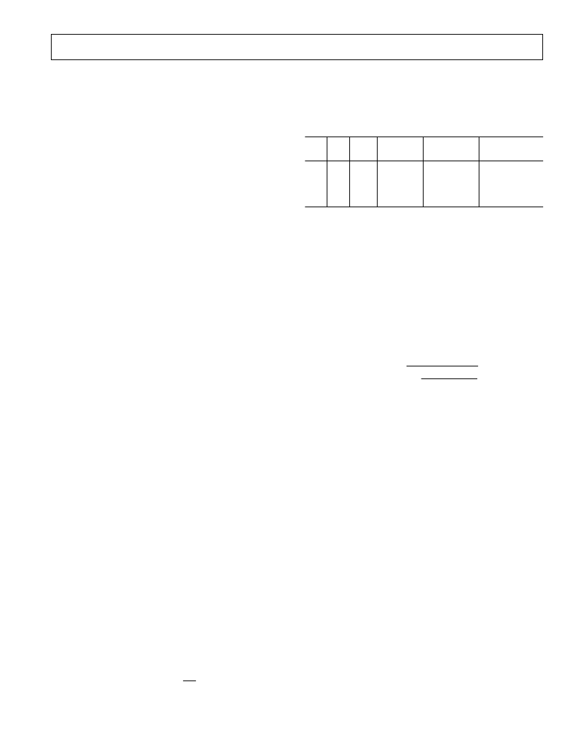
Table II. Recommended Resistor Values and
Noise Performance for Specific Gains
R
G
( ) ( )
R
F
Bandwidth Output Noise Output Noise
–3 dB
AD8132 Only AD8132 + R
G
, R
F
360 MHz
16 nV/
√
Hz
160 MHz
24.1 nV/
√
Hz
499 2.49 k 65 MHz
48.4 nV/
√
Hz
499 4.99 k 20 MHz
88.9 nV/
√
Hz
Gain
1
2
5
10
499 499
499 1.0 k
17 nV/
√
Hz
26.1 nV/
√
Hz
53.3 nV/
√
Hz
98.6 nV/
√
Hz
Calculating an Application Circuit’s Input Impedance
The effective input impedance of a circuit such as that in Fig-
ure 3, at +D
IN
and
–
D
IN
, will depend on whether the ampli
fi
er is
being driven by a single-ended or differential signal source. For
balanced differential input signals, the input impedance (R
IN
,dm)
between the inputs (+D
IN
and
–
D
IN
) is simply:
R
IN,dm
= 2
×
R
G
In the case of a single-ended input signal (for example if
–
D
IN
is
grounded and the input signal is applied to +D
IN
), the input
impedance becomes:
R
R
R
R
R
IN dm
,
G
F
G
F
=
×
+
(
)
1
2
The circuit
’
s input impedance is effectively higher than it would
be for a conventional op amp connected as an inverter because a
fraction of the differential output voltage appears at the inputs
as a common-mode signal, partially bootstrapping the voltage
across the input resistor R
G
.
Input Common-Mode Voltage Range in Single Supply
Applications
The AD8132 is optimized for level-shifting
“
ground
”
referenced
input signals. For a single-ended input this would imply, for
example, that the voltage at
–
D
IN
in Figure 3 would be zero
volts when the ampli
fi
er
’
s negative power supply voltage (at V
–
)
was also set to zero volts.
Setting the Output Common-Mode Voltage
The AD8132
’
s V
OCM
pin is internally biased at a voltage approxi-
mately equal to the midsupply point (average value of the voltages
on V+ and V
–
). Relying on this internal bias will result in an
output common-mode voltage that is within about 100 mV of
the expected value.
In cases where more accurate control of the output common-mode
level is required, it is recommended that an external source,
or resistor divider (with R
SOURCE
< 10K), be used. The output
common-mode offset speci
fi
ed on pages 2 and 3 assume the
V
OCM
input is driven by a low impedance voltage source.
相關(guān)PDF資料 |
PDF描述 |
|---|---|
| AD8132AR | Low-Cost, High-Speed Differential Amplifier |
| AD8132AR-REEL | Low-Cost, High-Speed Differential Amplifier |
| AD8132AR-REEL7 | Low-Cost, High-Speed Differential Amplifier |
| AD8132ARM | Low-Cost, High-Speed Differential Amplifier |
| AD8132ARM-REEL | Low-Cost, High-Speed Differential Amplifier |
相關(guān)代理商/技術(shù)參數(shù) |
參數(shù)描述 |
|---|---|
| AD8132WARMZ-R7 | 功能描述:IC DIFF AMP 350MHZ 8-MSOP RoHS:是 類別:集成電路 (IC) >> Linear - Amplifiers - Instrumentation 系列:- 產(chǎn)品培訓(xùn)模塊:Differential Circuit Design Techniques for Communication Applications 標(biāo)準(zhǔn)包裝:1 系列:- 放大器類型:RF/IF 差分 電路數(shù):1 輸出類型:差分 轉(zhuǎn)換速率:9800 V/µs 增益帶寬積:- -3db帶寬:2.9GHz 電流 - 輸入偏壓:3µA 電壓 - 輸入偏移:- 電流 - 電源:40mA 電流 - 輸出 / 通道:- 電壓 - 電源,單路/雙路(±):3 V ~ 3.6 V 工作溫度:-40°C ~ 85°C 安裝類型:表面貼裝 封裝/外殼:16-VQFN 裸露焊盤,CSP 供應(yīng)商設(shè)備封裝:16-LFCSP-VQ 包裝:剪切帶 (CT) 產(chǎn)品目錄頁面:551 (CN2011-ZH PDF) 其它名稱:ADL5561ACPZ-R7CT |
| AD8132WARMZ-R71,2 | 制造商:AD 制造商全稱:Analog Devices 功能描述:Low Cost, High Speed Differential Amplifier |
| AD8133 | 制造商:AD 制造商全稱:Analog Devices 功能描述:Triple Differential Driver With Output Pull-Down |
| AD8133ACP-R2 | 制造商:Rochester Electronics LLC 功能描述:TRIPLE DIFFEREN. DRIVER W/OUTPUT DISABLE - Bulk 制造商:Analog Devices 功能描述: |
| AD8133ACP-REEL | 制造商:Rochester Electronics LLC 功能描述: 制造商:Analog Devices 功能描述: |
發(fā)布緊急采購,3分鐘左右您將得到回復(fù)。