- 您現(xiàn)在的位置:買賣IC網(wǎng) > PDF目錄373938 > AD8132 (Analog Devices, Inc.) Low-Cost, High-Speed Differential Amplifier PDF資料下載
參數(shù)資料
| 型號: | AD8132 |
| 廠商: | Analog Devices, Inc. |
| 元件分類: | 運(yùn)動(dòng)控制電子 |
| 英文描述: | Low-Cost, High-Speed Differential Amplifier |
| 中文描述: | 低成本,高速差分放大器 |
| 文件頁數(shù): | 13/20頁 |
| 文件大小: | 391K |
| 代理商: | AD8132 |
REV. 0
AD8132
–13–
OPERATIONAL DESCRIPTION
Definition of Terms
AD8132
C
F
+IN
–
IN
R
F
C
F
R
F
R
G
R
G
+D
IN
V
OCM
–
D
IN
R
L, dm
+OUT
V
OUT, dm
–
OUT
Figure 3. Circuit Definitions
Differential voltage refers to the difference between two node
voltages. For example, the output differential voltage (or
equivalently output differential-mode voltage) is defined as:
V
OUT,dm
=
(
V
+OUT
– V
–OUT
)
V
+OUT
and
V
–OUT
refer to the voltages at the +OUT and –OUT
terminals with respect to a common reference.
Common-mode voltage refers to the average of two node volt-
ages. The output common-mode voltage is defined as:
V
OUT,cm
=
(
V
+OUT
+ V
–OUT
)
/
2
Basic Circuit Operation
One of the more useful and easy to understand ways to use the
AD8132 is to provide two equal-ratio feedback networks. To
match the effect of parasitics, these networks should actually be
comprised of two equal-value feedback resistors, R
F
and two
equal-value gain resistors, R
G
. This circuit is diagrammed in
Figure 3.
Like a conventional op amp, the AD8132 has two differential
inputs that can be driven with both a differential-mode input
voltage, V
IN,dm
, and a common-mode input voltage, V
IN,cm
.
There is another input, V
OCM
, which is not present on conven-
tional op amps, but provides another input to consider on the
AD8132. It is totally separate from the above inputs.
There are two complementary outputs whose response can be
defined by a differential-mode output, V
OUT,dm
and a common-
mode output, V
OUT,cm
.
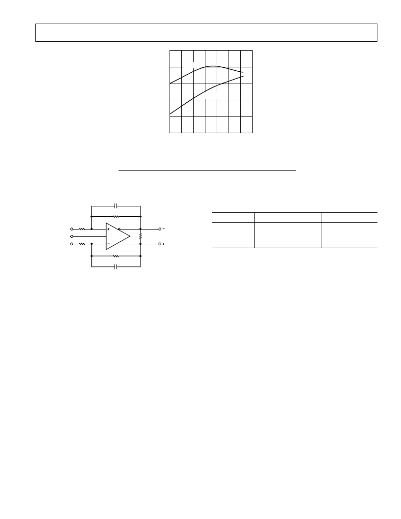
TEMPERATURE
–
C
D
–
0
–
0.5
–
2.5
–
40
–
20
100
0
20
40
60
80
–
1.0
–
1.5
–
2.0
V
S
= 5V
V
S
= 5V
TPC 59. Differential Offset Voltage vs. Temperature
Table I indicates the gain from any type of input to either type
of output.
Table I. Differential and Common-Mode Gains
Input
V
OUT,dm
R
F
/R
G
0
0
V
OUT,cm
0 (By Design)
0 (By Design)
1 (By Design)
V
IN,dm
V
IN,cm
V
OCM
The differential output (V
OUT,dm
) is equal to the differential
input voltage (V
IN,dm
) times R
F
/R
G
. In this case, it does not
matter if both differential inputs are driven, or only one output
is driven and the other is tied to a reference voltage, like ground.
As can be seen from the two zero entries in the first column,
neither of the common-mode inputs has any effect on this gain.
The gain from V
IN,dm
to V
OUT,cm
is 0 and to first order does not
depend on the ratio matching of the feedback networks. The
common-mode feedback loop within the AD8132 provides a
corrective action to keep this gain term minimized. The term
“balance error” describes the degree to which this gain term
differs from zero.
The gain from V
IN,cm
to V
OUT,dm
does directly depend on the
matching of the feedback networks. The analogous term for this
transfer function, which is used in conventional op amps, is
“common-mode rejection ratio” or CMRR. Thus, if it is desirable
to have a high CMRR, the feedback ratios must be well matched.
The gain from V
IN,cm
to V
OUT,cm
is also ideally 0, and is first-
order independent of the feedback ratio matching. As in the
case of V
IN,dm
to V
OUT,cm
, the common-mode feedback loop
keeps this term minimized.
The gain from V
OCM
to V
OUT,dm
is ideally 0 only when the feed-
back ratios are matched. The amount of differential output
signal that will be created by varying V
OCM
is related to the
degree of mismatch in the feedback networks.
V
OCM
controls the output common-mode voltage V
OUT,cm
with a
unity-gain transfer function. With equal-ratio feedback networks
(as assumed above), its effect on each output will be the same,
which is another way to say that the gain from V
OCM
to V
OUT,dm
is zero. If not driven, the output common-mode will be at mid-
supplies. It is recommended that a 0.1
μ
F bypass capacitor be
connected to V
OCM
.
相關(guān)PDF資料 |
PDF描述 |
|---|---|
| AD8132-EVAL | Low-Cost, High-Speed Differential Amplifier |
| AD8132AR | Low-Cost, High-Speed Differential Amplifier |
| AD8132AR-REEL | Low-Cost, High-Speed Differential Amplifier |
| AD8132AR-REEL7 | Low-Cost, High-Speed Differential Amplifier |
| AD8132ARM | Low-Cost, High-Speed Differential Amplifier |
相關(guān)代理商/技術(shù)參數(shù) |
參數(shù)描述 |
|---|---|
| AD8132_06 | 制造商:AD 制造商全稱:Analog Devices 功能描述:Low Cost, High Speed Differential Amplifier |
| AD8132_09 | 制造商:AD 制造商全稱:Analog Devices 功能描述:Low Cost, High Speed Differential Amplifier |
| AD8132AR | 功能描述:IC AMP DIFF LDIST LP 70MA 8SOIC RoHS:否 類別:集成電路 (IC) >> Linear - Amplifiers - Instrumentation 系列:- 標(biāo)準(zhǔn)包裝:73 系列:Over-The-Top® 放大器類型:通用 電路數(shù):4 輸出類型:滿擺幅 轉(zhuǎn)換速率:0.07 V/µs 增益帶寬積:200kHz -3db帶寬:- 電流 - 輸入偏壓:1nA 電壓 - 輸入偏移:285µV 電流 - 電源:50µA 電流 - 輸出 / 通道:25mA 電壓 - 電源,單路/雙路(±):2 V ~ 44 V,±1 V ~ 22 V 工作溫度:-40°C ~ 85°C 安裝類型:表面貼裝 封裝/外殼:16-WFDFN 裸露焊盤 供應(yīng)商設(shè)備封裝:16-DFN-EP(5x3) 包裝:管件 |
| AD8132AR | 制造商:Analog Devices 功能描述:SEMICONDUCTORS ((NW)) |
| AD8132AR-EBZ | 功能描述:BOARD EVAL FOR AD8132AR RoHS:是 類別:編程器,開發(fā)系統(tǒng) >> 評估板 - 運(yùn)算放大器 系列:- 產(chǎn)品培訓(xùn)模塊:Lead (SnPb) Finish for COTS Obsolescence Mitigation Program 標(biāo)準(zhǔn)包裝:1 系列:- |
發(fā)布緊急采購,3分鐘左右您將得到回復(fù)。