- 您現在的位置:買賣IC網 > PDF目錄5403 > AD8137YRZ-REEL7 (Analog Devices Inc)IC AMP DIFF R-R LP 20MA 8SOIC PDF資料下載
參數資料
| 型號: | AD8137YRZ-REEL7 |
| 廠商: | Analog Devices Inc |
| 文件頁數: | 1/33頁 |
| 文件大小: | 0K |
| 描述: | IC AMP DIFF R-R LP 20MA 8SOIC |
| 標準包裝: | 1,000 |
| 放大器類型: | 差分 |
| 電路數: | 1 |
| 輸出類型: | 差分,滿擺幅 |
| 轉換速率: | 450 V/µs |
| -3db帶寬: | 110MHz |
| 電流 - 輸入偏壓: | 500nA |
| 電壓 - 輸入偏移: | 700µV |
| 電流 - 電源: | 3.2mA |
| 電流 - 輸出 / 通道: | 20mA |
| 電壓 - 電源,單路/雙路(±): | 2.7 V ~ 12 V,± 2.7 V ~ 6 V |
| 工作溫度: | -40°C ~ 125°C |
| 安裝類型: | 表面貼裝 |
| 封裝/外殼: | 8-SOIC(0.154",3.90mm 寬) |
| 供應商設備封裝: | 8-SO |
| 包裝: | 帶卷 (TR) |
當前第1頁第2頁第3頁第4頁第5頁第6頁第7頁第8頁第9頁第10頁第11頁第12頁第13頁第14頁第15頁第16頁第17頁第18頁第19頁第20頁第21頁第22頁第23頁第24頁第25頁第26頁第27頁第28頁第29頁第30頁第31頁第32頁第33頁
Low Cost, Low Power,
Differential ADC Driver
Data Sheet
Rev. E
Information furnished by Analog Devices is believed to be accurate and reliable. However, no
responsibilityisassumedbyAnalogDevicesforitsuse,norforanyinfringementsofpatentsorother
rightsofthirdpartiesthatmayresultfromitsuse.Specificationssubjecttochangewithoutnotice.No
license is granted by implication or otherwise under any patent or patent rights of Analog Devices.
Trademarksandregisteredtrademarksarethepropertyoftheirrespectiveowners.
One Technology Way, P.O. Box 9106, Norwood, MA 02062-9106, U.S.A.
Tel: 781.329.4700
Fax: 781.461.3113
2004–2012 Analog Devices, Inc. All rights reserved.
FEATURES
Fully differential
Extremely low power with power-down feature
2.6 mA quiescent supply current @ 5 V
450 A in power-down mode @ 5 V
High speed
110 MHz large signal 3 dB bandwidth @ G = 1
450 V/s slew rate
12-bit SFDR performance @ 500 kHz
Fast settling time: 100 ns to 0.02%
Low input offset voltage: ±2.6 mV max
Low input offset current: 0.45 A max
Differential input and output
Differential-to-differential or single-ended-to-differential
operation
Rail-to-rail output
Adjustable output common-mode voltage
Externally adjustable gain
Wide supply voltage range: 2.7 V to 12 V
Available in small SOIC package
Qualified for automotive applications
APPLICATIONS
ADC drivers
Automotive vision and safety systems
Automotive infotainment systems
Portable instrumentation
Battery-powered applications
Single-ended-to-differential converters
Differential active filters
Video amplifiers
Level shifters
FUNCTIONAL BLOCK DIAGRAM
04771-0-001
–IN
1
VOCM 2
VS+ 3
+OUT
4
+IN
8
PD
7
VS–
6
–OUT
5
AD8137
Figure 1.
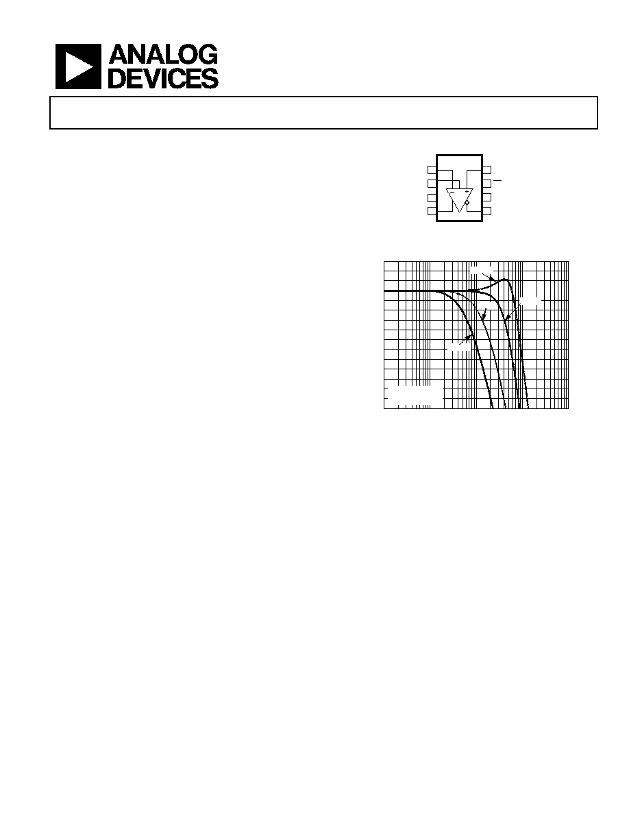
RG = 1k
VO, dm = 0.1V p-p
FREQUENCY (MHz)
NORMALIZED
CLOSED-LOOP
GAIN
(dB)
3
2
1
0
–12
–11
–10
–9
–8
–7
–6
–5
–4
–3
–2
–1
0.1
1
10
100
1000
04771-0-002
G = 5
G = 10
G = 1
G = 2
Figure 2. Small Signal Response for Various Gains
GENERAL DESCRIPTON
The AD8137 is a low cost differential driver with a rail-to-rail
output that is ideal for driving ADCs in systems that are sensitive
to power and cost. The AD8137 is easy to apply, and its internal
common-mode feedback architecture allows its output common-
mode voltage to be controlled by the voltage applied to one pin.
The internal feedback loop also provides inherently balanced
outputs as well as suppression of even-order harmonic distortion
products. Fully differential and single-ended-to-differential gain
configurations are easily realized by the AD8137. External
feedback networks consisting of four resistors determine the
closed-loop gain of the amplifier. The power-down feature is
beneficial in critical low power applications.
The AD8137 is manufactured on Analog Devices, Inc.,
proprietary second-generation XFCB process, enabling it to
achieve high levels of performance with very low power
consumption.
The AD8137 is available in the small 8-lead SOIC package and
3 mm × 3 mm LFCSP package. It is rated to operate over the
extended industrial temperature range of 40°C to +125°C.
相關PDF資料 |
PDF描述 |
|---|---|
| LTC2054HVCS5#TRMPBF | IC OPAMP 0-DRIFT SGL LP TSOT23-5 |
| LTC2054HVCS5#TRM | IC OPAMP 0-DRIFT SGL LP TSOT23-5 |
| AD822ARMZ-R2 | IC OPAMP GP R-R 1.9MHZ LP 8MSOP |
| LTC2054HVCS5#TRPBF | IC OPAMP 0-DRIFT SGL LP TSOT23-5 |
| TSW-125-26-L-D | CONN HEADER 50POS .100" DL GOLD |
相關代理商/技術參數 |
參數描述 |
|---|---|
| AD8138 | 制造商:AD 制造商全稱:Analog Devices 功能描述:Low Distortion Differential ADC Driver |
| AD8138_06 | 制造商:AD 制造商全稱:Analog Devices 功能描述:Low Distortion Differential ADC Driver |
| AD81380703L | 制造商:Analog Devices 功能描述: |
| AD8138AAR-EBZ | 功能描述:BOARD EVAL FOR AD8138AAR RoHS:是 類別:編程器,開發系統 >> 評估板 - 運算放大器 系列:- 產品培訓模塊:Lead (SnPb) Finish for COTS Obsolescence Mitigation Program 標準包裝:1 系列:- |
| AD8138AARMZ | 功能描述:IC DIFF ADC DVR LOW DISTOR 8MSOP RoHS:是 類別:集成電路 (IC) >> 線性 - 放大器 - 專用 系列:- 產品培訓模塊:Lead (SnPb) Finish for COTS Obsolescence Mitigation Program 標準包裝:60 系列:- 類型:可變增益放大器 應用:CATV 安裝類型:表面貼裝 封裝/外殼:20-WQFN 裸露焊盤 供應商設備封裝:20-TQFN-EP(5x5) 包裝:托盤 |
發布緊急采購,3分鐘左右您將得到回復。