- 您現在的位置:買賣IC網 > PDF目錄373938 > AD8139ACP-R2 (ANALOG DEVICES INC) Low Noise Rail-to-Rail Differential ADC Driver PDF資料下載
參數資料
| 型號: | AD8139ACP-R2 |
| 廠商: | ANALOG DEVICES INC |
| 元件分類: | 運動控制電子 |
| 英文描述: | Low Noise Rail-to-Rail Differential ADC Driver |
| 中文描述: | OP-AMP, 500 uV OFFSET-MAX, DSO8 |
| 封裝: | 3 X 3 MM, LFCSP-8 |
| 文件頁數: | 21/24頁 |
| 文件大小: | 720K |
| 代理商: | AD8139ACP-R2 |
AD8139
The circuit has a differential gain of 1.6 and β = 0.38.
V
ICM
has
an amplitude of 2.5 V p-p and is swinging about ground. Using
the results in Equation 16, the common-mode voltage at the
AD8139’s inputs,
V
ACM
, is a 1.5 V p-p signal swinging about a
baseline of 0.95 V. The maximum negative excursion of
V
ACM
in
this case is 0.2 V, which exceeds the lower input common-mode
voltage limit.
Rev. A | Page 21 of 24
One way to avoid the input common-mode swing limitation is
to bias V
IN
and V
REF
at midsupply. In this case,
V
IN
is 5 V p-p
swinging about a baseline at 2.5 V and V
REF
is connected to a
low-Z 2.5 V source. V
ICM
now has an amplitude of 2.5 V p-p and
is swinging about 2.5 V. Using the results in Equation 17,
V
ACM
is
calculated to be equal to
V
ICM
because
V
OCM
=
V
ICM
. Therefore,
V
ACM
swings from 1.25 V to 3.75 V, which is well within the
input common-mode voltage limits of the AD8139. Another
benefit seen in this example is that since
V
OCM
=
V
ACM
=
V
ICM
no
wasted common-mode current flows. Figure 60 illustrates how
to provide the low-Z bias voltage. For situations that do not
require a precise reference, a simple voltage divider will suffice
to develop the input voltage to the buffer.
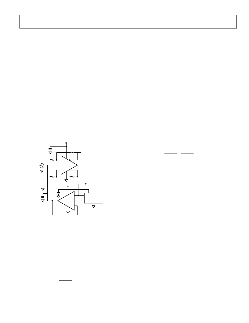
0
V
IN
0V TO 5V
AD8139
+
–
8
2
1
6
3
4
5
V
OCM
200
324
5V
200
324
0.1
μ
F
0.1
μ
F
10
μ
F
+
AD8031
+
–
0.1
μ
F
5V
ADR431
2.5V
REFERENCE
TO AD7674 REFBUFIN
Figure 60. Low-Z 2.5 V Buffer
Another way to avoid the input common-mode swing limita-
tion is to use dual power supplies on the AD8139. In this case,
the biasing circuitry is not required.
Bandwidth Versus Closed-Loop Gain
The AD8139’s 3 dB bandwidth decreases proportionally to
increasing closed-loop gain in the same way as a traditional
voltage feedback operational amplifier. For closed-loop gains
greater than 4, the bandwidth obtained for a specific gain can be
estimated as
)
300
(
,
3
,
MHz
R
R
R
V
dB
f
F
G
G
dm
OUT
×
+
=
(20)
or equivalently, β(300 MHz).
This estimate assumes a minimum 90 degree phase margin for
the amplifier loop, which is a condition approached for gains
greater than 4. Lower gains will show more bandwidth than
predicted by the equation due to the peaking produced by the
lower phase margin.
Estimating DC Errors
Primary differential output offset errors in the AD8139 are due
to three major components: the input offset voltage, the offset
between the V
AN
and V
AP
input currents interacting with the
feedback network resistances, and the offset produced by the dc
voltage difference between the input and output common-mode
voltages in conjunction with matching errors in the feedback
network.
The first output error component is calculated as
+
R
=
G
G
F
IO
R
R
V
e
Vo
1
_
, or equivalently as V
IO
/β
(21)
where V
IO
is the input offset voltage. The input offset voltage of the
AD8139 is laser trimmed and guaranteed to be less than 500 μV
The second error is calculated as
(
)
F
IO
G
F
F
R
G
+
G
G
F
IO
R
I
R
R
R
R
R
R
I
e
Vo
=
+
=
2
_
(22)
where I
IO
is defined as the offset between the two input bias
currents.
The third error voltage is calculated as
)
(
3
_
OCM
V
ICM
V
enr
e
Vo
×
=
(23)
where Δ
enr
is the fractional mismatch between the two
feedback resistors.
The total differential offset error is the sum of these three error
sources.
Other Impact of Mismatches in the Feedback Networks
The internal common-mode feedback network will still force
the output voltages to remain balanced, even when the R
F
/R
G
feedback networks are mismatched. The mismatch will,
however, cause a gain error proportional to the feedback
network mismatch.
Ratio-matching errors in the external resistors will degrade the
ability to reject common-mode signals at the V
AN
and V
IN
input
terminals, much the same as with a four-resistor difference
amplifier made from a conventional op amp. Ratio-matching
errors will also produce a differential output component that is
equal to the V
OCM
input voltage times the difference between the
feedback factors (βs). In most applications using 1% resistors,
this component amounts to a differential dc offset at the output
that is small enough to be ignored.
相關PDF資料 |
PDF描述 |
|---|---|
| AD8139ACPZ-REEL | Low Noise Rail-to-Rail Differential ADC Driver |
| AD8146 | Triple Differential Driver for Wideband Video |
| AD8146ACPZ-R2 | Triple Differential Driver for Wideband Video |
| AD8146ACPZ-R7 | Triple Differential Driver for Wideband Video |
| AD8146ACPZ-RL | Triple Differential Driver for Wideband Video |
相關代理商/技術參數 |
參數描述 |
|---|---|
| AD8139ACP-REEL | 制造商:Analog Devices 功能描述:SP Amp DIFF AMP Single R-R O/P ±6V/12V 8-Pin LFCSP EP T/R |
| AD8139ACP-REEL7 | 制造商:Analog Devices 功能描述:SP Amp DIFF AMP Single R-R O/P ±6V/12V 8-Pin LFCSP EP T/R 制造商:Rochester Electronics LLC 功能描述: |
| AD8139ACPZ | 制造商:Analog Devices 功能描述:Amplifier, Diff,ADC Driver,AD8139ACPZ |
| AD8139ACPZ-R2 | 制造商:Analog Devices 功能描述:SP Amp DIFF AMP Single R-R O/P ±6V/12V 8-Pin LFCSP EP T/R 制造商:Analog Devices 功能描述:HIGH PERFORMANCE LOW NOISE ADC DRIVER - Tape and Reel 制造商:Analog Devices 功能描述:5V to 12V 1 410MHz IyAv 8LFCSP AiOEfoCZY Tape & Reel 制造商:Analog Devices 功能描述:IC ADC DRIVER SMD 8139 LFCSP-8 制造商:Analog Devices 功能描述:IC, ADC, DRIVER, SMD, 8139, LFCSP-8 制造商:Analog Devices 功能描述:Differential ADC Driver Low Noise LFCSP8 |
| AD8139ACPZ-R21 | 制造商:AD 制造商全稱:Analog Devices 功能描述:Low Noise Rail-to-Rail Differential ADC Driver |
發布緊急采購,3分鐘左右您將得到回復。