- 您現(xiàn)在的位置:買賣IC網(wǎng) > PDF目錄373939 > AD8150 (Analog Devices, Inc.) 33 x 17, 1.5 Gbps Digital Crosspoint Switch PDF資料下載
參數(shù)資料
| 型號: | AD8150 |
| 廠商: | Analog Devices, Inc. |
| 英文描述: | 33 x 17, 1.5 Gbps Digital Crosspoint Switch |
| 中文描述: | 33 × 17,1.5 Gbps的數(shù)字交叉點(diǎn)開關(guān) |
| 文件頁數(shù): | 19/35頁 |
| 文件大小: | 995K |
| 代理商: | AD8150 |
第1頁第2頁第3頁第4頁第5頁第6頁第7頁第8頁第9頁第10頁第11頁第12頁第13頁第14頁第15頁第16頁第17頁第18頁當(dāng)前第19頁第20頁第21頁第22頁第23頁第24頁第25頁第26頁第27頁第28頁第29頁第30頁第31頁第32頁第33頁第34頁第35頁
AD8150
–19–
REV. 0
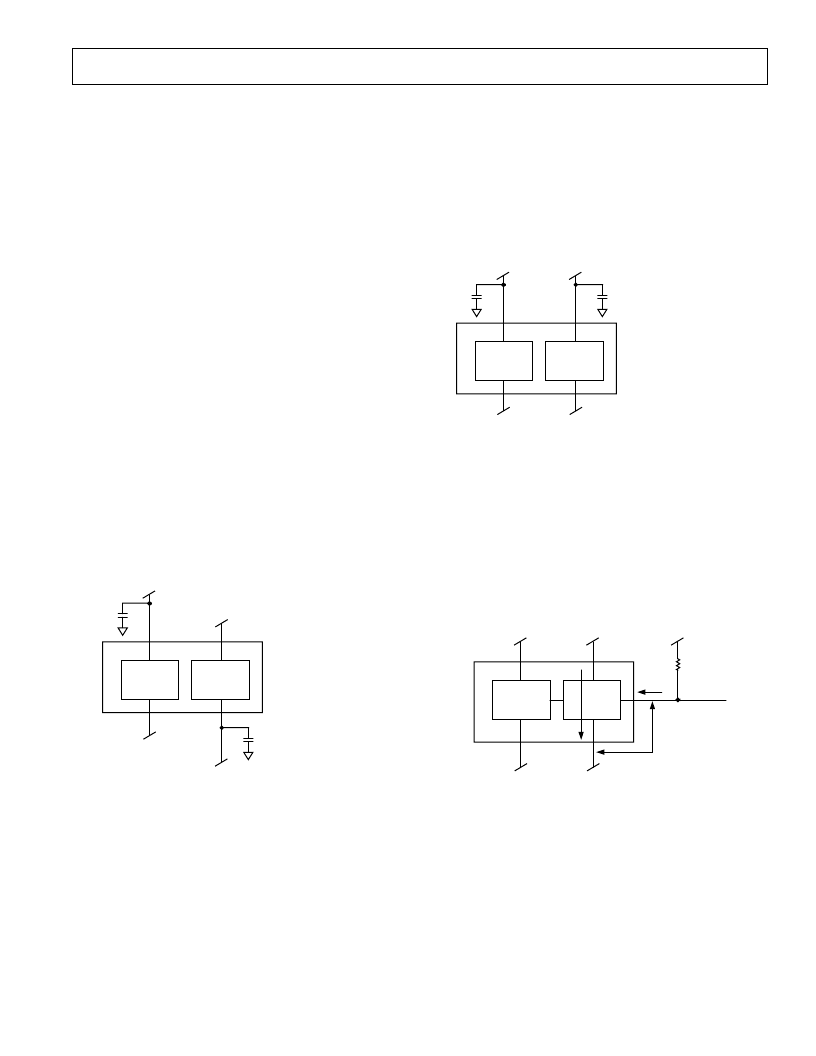
Power Supplies
There are several options for the power supply voltages for the
AD8150, as there are two separate sections of the chip that require
power supplies. These are the control logic and the high-speed
data paths. Depending on the system architecture, the voltage
levels of these supplies can vary.
Logic Supplies
The control (programming) logic is CMOS and is designed to
interface with any of the various standard single-ended logic
families (CMOS or TTL). Its supply voltage pins are V
DD
(Pin
170, logic positive) and V
SS
(Pin 152, logic ground). In all cases
the logic ground should be connected to the system digital ground.
V
DD
should be supplied at between 3.3 V to 5 V to match the
supply voltage of the logic family that is used to drive the logic
inputs. V
DD
should be bypassed to ground with a 0.1
μ
F ceramic
capacitor. The absolute maximum voltage from V
DD
to V
SS
is 5.5 V.
Data Path Supplies
The data path supplies have more options for their voltage lev-
els. The choices here will affect several other areas, like power
dissipation, bypassing, and common mode levels of the inputs
and outputs. The more positive voltage supply for the data paths
is V
CC
(Pins 41, 98, 149 and 171). The more negative supply is
V
EE
, which appears on many pins that will not be listed here.
The maximum allowable voltage across these supplies is 5.5 V.
The
fi
rst choice in the data path power supplies is to decide
whether to run the device as ECL (Emitter-Coupled Logic) or
PECL (Positive ECL). For ECL operation, V
CC
will be at ground
potential, while V
EE
will be at a negative supply between
–
3.3 V
to
–
5 V. This will make the common-mode voltage of the inputs
and outputs at a negative voltage, see Figure 37.
DATA
PATHS
CONTROL
LOGIC
3V TO 5V
3V TO 5V
V
SS
V
EE
GND
GND
0.1 F
(ONE FOR EVERY TWO V
EE
PINS)
0.1 F
AD8150
V
DD
V
CC
Figure 37. Power Supplies and Bypassing for ECL
Operation
If the data paths are to be dc-coupled to other ECL logic devices
that run with ground as the most positive supply and a negative
voltage for V
EE
, then this is the proper way to run. However, if
the part is to be ac coupled, it is not necessary to have the input/
output common mode at the same level as the other system cir-
cuits, but it will probably be more convenient to use the same
supply rails for all devices.
For PECL operation, V
EE
will be at ground potential and V
CC
will be a positive voltage from 3.3 V to 5 V. Thus, the common
mode of the inputs and outputs will be at a positive voltage.
These can then be dc coupled to other PECL operated devices.
If the data paths are ac coupled, then the common-mode levels
do not matter, see Figure 38.
DATA
PATHS
CONTROL
LOGIC
3V TO 5V
3V TO 5V
V
SS
V
EE
GND
GND
0.1 F
(ONE FOR EACH V
CC
PIN, 4 REQ'D.)
0.1 F
AD8150
V
DD
V
CC
Figure 38. Power Supplies and Bypassing for PECL
Operation
POWER DISSIPATION
For analysis, the power dissipation of the AD8150 can be divided
into three separate parts. These are the control logic, the data
path circuits and the (ECL or PECL) outputs, which are part of
the data path circuits, but can be dealt with separately. The
fi
rst
of these, the control logic, is CMOS technology and does not
dissipate a signi
fi
cant amount of power. This power will, of
course, be greater when the logic supply is 5 V rather than 3 V,
but overall it is not a signi
fi
cant amount of power and can be
ignored for thermal analysis.
DATA
PATHS
CONTROL
LOGIC
V
SS
V
EE
GND
GND
AD8150
V
DD
V
CC
I, DATA PATH
LOGIC
V
OUT
LOW
–
V
EE
R
OUT
I
OUT
Figure 39. Major Power Consumption Paths
The data path circuits operate between the supplies V
CC
and
V
EE
. As described in the power supply section, this voltage can
range from 3.3 V to 5 V. The current consumed by this section
will be constant, so operating at a lower voltage can save about
40 percent in power dissipation.
相關(guān)PDF資料 |
PDF描述 |
|---|---|
| AD8150AST | 33 x 17, 1.5 Gbps Digital Crosspoint Switch |
| AD8151-EVAL | GPA/SK 300X280X1,5... |
| AD8151 | 33 x 17, 3.2 Gb/s Digital Crosspoint Switch |
| AD8151AST | 33 x 17, 3.2 Gb/s Digital Crosspoint Switch |
| AD8156 | 6.25 Gbps 4】4 Digital Crosspoint Switch with EQ |
相關(guān)代理商/技術(shù)參數(shù) |
參數(shù)描述 |
|---|---|
| AD8150AST | 制造商:Rochester Electronics LLC 功能描述:LQFP 1.5GBPS 33X17 DIGITAL CROSSPOINT SW - Tape and Reel 制造商:Analog Devices 功能描述:IC SWITCH CROSSPOINT |
| AD8150ASTZ | 功能描述:IC CROSSPOINT SWIT 33X17 184LQFP RoHS:是 類別:集成電路 (IC) >> 接口 - 模擬開關(guān),多路復(fù)用器,多路分解器 系列:XStream™ 應(yīng)用說明:Ultrasound Imaging Systems Application Note 產(chǎn)品培訓(xùn)模塊:Lead (SnPb) Finish for COTS Obsolescence Mitigation Program 標(biāo)準(zhǔn)包裝:250 系列:- 功能:開關(guān) 電路:單刀單擲 導(dǎo)通狀態(tài)電阻:48 歐姆 電壓電源:單電源 電壓 - 電源,單路/雙路(±):2.7 V ~ 5.5 V 電流 - 電源:5µA 工作溫度:0°C ~ 70°C 安裝類型:表面貼裝 封裝/外殼:48-LQFP 供應(yīng)商設(shè)備封裝:48-LQFP(7x7) 包裝:托盤 |
| AD8150ASTZ | 制造商:Analog Devices 功能描述:IC DIGITAL CROSSPOINT SWITCH |
| AD8150-EVAL | 制造商:Analog Devices 功能描述:EVAL KIT FOR 33 17, 1.5 GBPS DGTL CROSSPOINT SWIT - Bulk |
| AD8151 | 制造商:AD 制造商全稱:Analog Devices 功能描述:33 x 17, 3.2 Gb/s Digital Crosspoint Switch |
發(fā)布緊急采購,3分鐘左右您將得到回復(fù)。