- 您現在的位置:買賣IC網 > PDF目錄373939 > AD815 (Electronic Theatre Controls, Inc.) SILICON DUAL DIFFERNTIAL AMPLIFIER TRANSISTORS PDF資料下載
參數資料
| 型號: | AD815 |
| 廠商: | Electronic Theatre Controls, Inc. |
| 英文描述: | SILICON DUAL DIFFERNTIAL AMPLIFIER TRANSISTORS |
| 中文描述: | 硅晶體管放大器雙DIFFERNTIAL |
| 文件頁數: | 10/16頁 |
| 文件大小: | 333K |
| 代理商: | AD815 |
AD815
REV. B
–10–
Choice of Feedback and Gain Resistors
The fine scale gain flatness will, to some extent, vary with
feedback resistance. It therefore is recommended that once
optimum resistor values have been determined, 1% tolerance
values should be used if it is desired to maintain flatness over
a wide range of production lots. Table I shows optimum values
for several useful configurations. These should be used as
starting point in any application.
Table I. Resistor Values
R
F
(
V
)
562
499
499
499
1 k
R
G
(
V
)
G =
+1
–1
+2
+5
+10
`
499
499
125
110
PRINTED CIRCUIT BOARD LAYOUT
CONSIDERATIONS
As to be expected for a wideband amplifier, PC board parasitics
can affect the overall closed-loop performance. Of concern are
stray capacitances at the output and the inverting input nodes. If
a ground plane is to be used on the same side of the board as
the signal traces, a space (5 mm min) should be left around the
signal lines to minimize coupling.
POWER SUPPLY BYPASSING
Adequate power supply bypassing can be critical when optimizing
the performance of a high frequency circuit. Inductance in the
power supply leads can form resonant circuits that produce
peaking in the amplifier’s response. In addition, if large current
transients must be delivered to the load, then bypass capacitors
(typically greater than 1
μ
F) will be required to provide the best
settling time and lowest distortion. A parallel combination of
10.0
μ
F and 0.1
μ
F is recommended. Under some low frequency
applications, a bypass capacitance of greater than 10
μ
F may be
necessary. Due to the large load currents delivered by the
AD815, special consideration must be given to careful bypassing.
The ground returns on both supply bypass capacitors as well as
signal common must be “star” connected as shown in Figure 41.
R
F
R
G
(OPTIONAL)
R
F
+V
S
+OUT
–OUT
–V
S
+IN
–IN
Figure 41. Signal Ground Connected in “Star”
Configuration
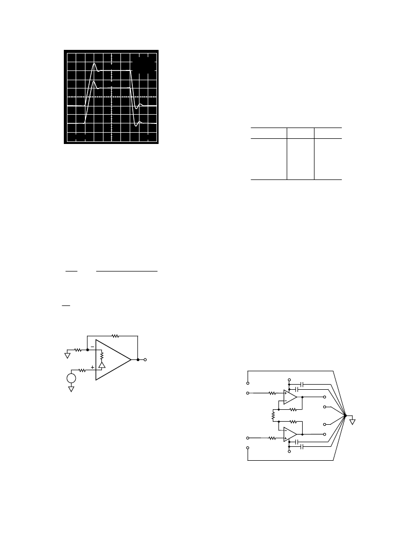
1V
20ns
SIDE B
SIDE A
G = –1
R
F
= 562
V
R
L
= 100
V
Figure 39. 4 V Step Response, G = –1
THEORY OF OPERATION
The AD815 is a dual current feedback amplifier with high
(500 mA) output current capability. Being a current feedback
amplifier, the AD815’s open-loop behavior is expressed
as transimpedance,
V
O
/
I
–IN
, or T
Z
. The open-loop
transimpedance behaves just as the open-loop voltage gain
of a voltage feedback amplifier, that is, it has a large dc value
and decreases at roughly 6 dB/octave in frequency.
Since R
IN
is proportional to 1/g
M
, the equivalent voltage gain is
just T
Z
×
g
M
, where the g
M
in question is the transconductance
of the input stage. Using this amplifier as a follower with gain,
Figure 40, basic analysis yields the following result:
V
O
V
IN
=
G
×
T
Z
S
( )
T
Z
S
( )
+
G
×
R
IN
+
R
F
where:
R
IN
= 1/
g
M
≈
25
G
R
R
F
G
=
+
1
R
IN
V
IN
R
F
V
OUT
R
G
R
N
Figure 40. Current Feedback Amplifier Operation
Recognizing that G
×
R
IN
<< R
F
for low gains, it can be seen to
the first order that bandwidth for this amplifier is independent
of gain (G).
Considering that additional poles contribute excess phase at
high frequencies, there is a minimum feedback resistance below
which peaking or oscillation may result. This fact is used to
determine the optimum feedback resistance, R
F
. In practice
parasitic capacitance at the inverting input terminal will also add
phase in the feedback loop, so picking an optimum value for R
F
can be difficult.
Achieving and maintaining gain flatness of better than 0.1 dB at
frequencies above 10 MHz requires careful consideration of
several issues.
相關PDF資料 |
PDF描述 |
|---|---|
| AD815ARB-24-REEL | High Output Current Differential Driver |
| AD815-EB | High Output Current Differential Driver |
| AD815AVR | High Output Current Differential Driver |
| AD815AY | High Output Current Differential Driver |
| AD815AYS | High Output Current Differential Driver |
相關代理商/技術參數 |
參數描述 |
|---|---|
| AD815_05 | 制造商:AD 制造商全稱:Analog Devices 功能描述:High Output Current Differential Driver |
| AD8150 | 制造商:AD 制造商全稱:Analog Devices 功能描述:33 x 17, 1.5 Gbps Digital Crosspoint Switch |
| AD8150AST | 制造商:Rochester Electronics LLC 功能描述:LQFP 1.5GBPS 33X17 DIGITAL CROSSPOINT SW - Tape and Reel 制造商:Analog Devices 功能描述:IC SWITCH CROSSPOINT |
| AD8150ASTZ | 功能描述:IC CROSSPOINT SWIT 33X17 184LQFP RoHS:是 類別:集成電路 (IC) >> 接口 - 模擬開關,多路復用器,多路分解器 系列:XStream™ 應用說明:Ultrasound Imaging Systems Application Note 產品培訓模塊:Lead (SnPb) Finish for COTS Obsolescence Mitigation Program 標準包裝:250 系列:- 功能:開關 電路:單刀單擲 導通狀態電阻:48 歐姆 電壓電源:單電源 電壓 - 電源,單路/雙路(±):2.7 V ~ 5.5 V 電流 - 電源:5µA 工作溫度:0°C ~ 70°C 安裝類型:表面貼裝 封裝/外殼:48-LQFP 供應商設備封裝:48-LQFP(7x7) 包裝:托盤 |
| AD8150ASTZ | 制造商:Analog Devices 功能描述:IC DIGITAL CROSSPOINT SWITCH |
發布緊急采購,3分鐘左右您將得到回復。