- 您現(xiàn)在的位置:買(mǎi)賣(mài)IC網(wǎng) > PDF目錄373939 > AD8174AN (ANALOG DEVICES INC) 250 MHz, 10 ns Switching Multiplexers w/Amplifier PDF資料下載
參數(shù)資料
| 型號(hào): | AD8174AN |
| 廠(chǎng)商: | ANALOG DEVICES INC |
| 元件分類(lèi): | 運(yùn)動(dòng)控制電子 |
| 英文描述: | 250 MHz, 10 ns Switching Multiplexers w/Amplifier |
| 中文描述: | 4-CHANNEL, VIDEO MULTIPLEXER, PDIP14 |
| 封裝: | PLASTIC, DIP-14 |
| 文件頁(yè)數(shù): | 8/16頁(yè) |
| 文件大小: | 474K |
| 代理商: | AD8174AN |
第1頁(yè)第2頁(yè)第3頁(yè)第4頁(yè)第5頁(yè)第6頁(yè)第7頁(yè)當(dāng)前第8頁(yè)第9頁(yè)第10頁(yè)第11頁(yè)第12頁(yè)第13頁(yè)第14頁(yè)第15頁(yè)第16頁(yè)
AD8170/AD8174
–8–
REV. 0
THEORY OF OPERATION
General
The AD8170/AD8174 multiplexers integrate wideband analog
switches with a high speed current feedback amplifier. The
input switches are complementary bipolar follower stages that
are turned on and off by using a current steering technique that
attains switch times of less than 10 ns and ensures low switching
transients. The 250 MHz current feedback amplifier provides
up to 50 mA of drive current. Overall gain and frequency
response are set by external resistors for maximum versatility.
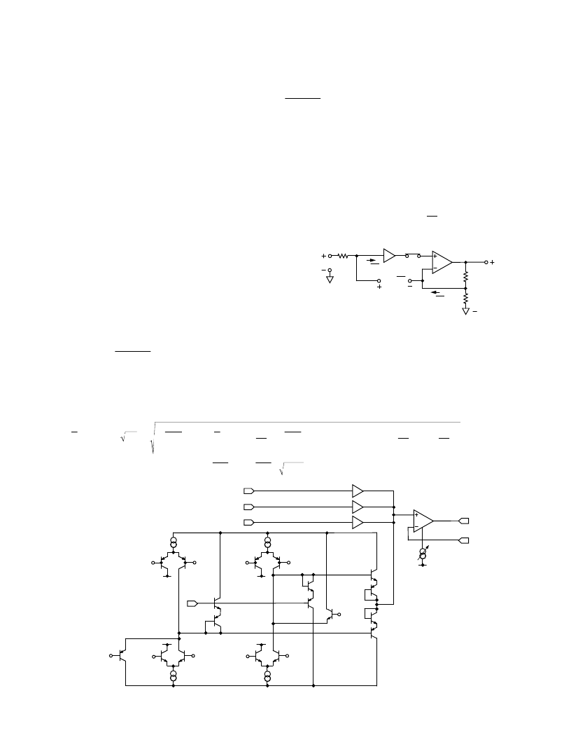
Figure 22 is a block diagram of the multiplexer signal chain,
with a simplified schematic of an input switch. When the
channel is on (i.e., V
ONB
more positive than V
REFB
, V
ONT
more
negative than V
REFT
), I2 flows through Q1 and Q2, and I3 flows
through Q3 and Q4. This biases up Q5 through Q8 to form the
unity gain follower. I1 and I4 (the “off” currents) are steered,
either to another switch or to the power supply. When the
channel turns off, I2 and I3 are steered away while I1 switches
over to pull the base of Q8 up to V
CLT
+ 1 V
BE
(about 2.7 volts
from ground reference) and I4 switches over to pull the base of
Q5 down to V
CLB
– 1 V
BE
(about –2.7 volts away from ground
reference). Clamping the bases of the reverse biased output
transistors to a low impedance point greatly improves isolation
performance.
The AD8174 has four switches with outputs wired together and
driving the positive input of a current feedback amplifier to form
a 4:1 multiplexer. It is designed so that only one channel is on
at a time. By bringing
ENABLE
high, the supply current for the
amplifier is shut off. This turns the output of the amplifier into
a high impedance, allowing the AD8174 to be used in larger
arrays. In practice, the disabled output impedance of the mux
will be determined by the amplifier’s feedback network.
Bringing SD high shuts off the supply current for all the switches,
that some of the logic control circuitry and the amplifier,
reducing the quiescent current drain to 1.5 mA. If the
ENABLE
and SD functions are not to be used, those respective
pins must be tied to ground for proper operation. Any unused
channel input should also be tied to ground.
The AD8170 has two switches driving an amplifier to form a 2:1
multiplexer. No disable or shutdown functions are provided.
DC Performance and Noise Considerations
Figure 23 shows the different contributors to total output offset
and noise. Total expected output offset can be calculated using
Equation 1 below:
V
OS
out
(
)
=
I
B
+
×
R
S
(
)
+
V
OS
[
]
1
+
R
F
R
G
+
I
B
×
R
F
(
)
(1)
V
OS
/V
en
I
B+
/I
en+
R
S
V
IN
SWITCH
BUFFER
I
B–
/I
en–
R
F
R
G
V
OUT
Figure 23. DC Errors for Buffered Multiplexer
Equations 2 and 3 below can be used to predict the output
voltage noise of the multiplexer for different choices of gains
and external resistors. The different contributions to output
noise are root-sum-squared to calculate total output noise
spectral density in Equation 2. As there is no peaking in the
multiplier’s noise characteristic, the total peak-to-peak output
noise will be accurately predicted using Equation 3.
V
EN
(
OUT
)
nV
/
Hz
(
)
=
I
EN
+
×
R
S
(
)
2
+
V
EN
(
)
2
1
+
R
F
R
G
2
+
I
EN
–
×
R
F
(
)
2
+
4
KT R
F
+
R
S
1
+
R
F
R
G
2
+
R
G
R
F
R
G
2
(2)
V
EN
p
p
=
V
EN
×
f
3
dB
×
6.2
×
1.26
(3)
VOUT
VFB
I6
I3
VCLB
VONT
VREFT
VOFFB
VREFB
VOFFT
VREFT
I1
VONB
VREFB
I4
I2
VCLT
IN0
IN1
IN2
IN3
Q1
Q2
Q3
Q4
Q5
Q6
Q7
Q8
Figure 22. Block Diagram and Simplified Schematic of the AD8170
相關(guān)PDF資料 |
PDF描述 |
|---|---|
| AD8174AR | 250 MHz, 10 ns Switching Multiplexers w/Amplifier |
| AD8174AR-REEL | VARISTOR 11VRMS 20MM RADIAL |
| AD8170 | 250 MHz, 10 ns Switching Multiplexers w/Amplifier(高速緩沖多路復(fù)用器) |
| AD8174 | 250 MHz, 10 ns Switching Multiplexers w/Amplifier(高速緩沖多路復(fù)用器) |
| AD8175 | Video Crosspoint Switch |
相關(guān)代理商/技術(shù)參數(shù) |
參數(shù)描述 |
|---|---|
| AD8174ANZ | 功能描述:IC MUX SW W/AMP 250MHZ 14-DIP RoHS:是 類(lèi)別:集成電路 (IC) >> 接口 - 專(zhuān)用 系列:- 特色產(chǎn)品:NXP - I2C Interface 標(biāo)準(zhǔn)包裝:1 系列:- 應(yīng)用:2 通道 I²C 多路復(fù)用器 接口:I²C,SM 總線(xiàn) 電源電壓:2.3 V ~ 5.5 V 封裝/外殼:16-TSSOP(0.173",4.40mm 寬) 供應(yīng)商設(shè)備封裝:16-TSSOP 包裝:剪切帶 (CT) 安裝類(lèi)型:表面貼裝 產(chǎn)品目錄頁(yè)面:825 (CN2011-ZH PDF) 其它名稱(chēng):568-1854-1 |
| AD8174AR | 功能描述:IC MUX W/AMP BUFFERED 14-SOIC RoHS:否 類(lèi)別:集成電路 (IC) >> 接口 - 專(zhuān)用 系列:- 特色產(chǎn)品:NXP - I2C Interface 標(biāo)準(zhǔn)包裝:1 系列:- 應(yīng)用:2 通道 I²C 多路復(fù)用器 接口:I²C,SM 總線(xiàn) 電源電壓:2.3 V ~ 5.5 V 封裝/外殼:16-TSSOP(0.173",4.40mm 寬) 供應(yīng)商設(shè)備封裝:16-TSSOP 包裝:剪切帶 (CT) 安裝類(lèi)型:表面貼裝 產(chǎn)品目錄頁(yè)面:825 (CN2011-ZH PDF) 其它名稱(chēng):568-1854-1 |
| AD8174AR-REEL | 制造商:Analog Devices 功能描述:Analog Multiplexer/Amp Single 4:1 14-Pin SOIC N T/R |
| AD8174AR-REEL7 | 功能描述:IC MUX SWITCHNG W/AMP 4:1 14SOIC RoHS:否 類(lèi)別:集成電路 (IC) >> 接口 - 專(zhuān)用 系列:- 特色產(chǎn)品:NXP - I2C Interface 標(biāo)準(zhǔn)包裝:1 系列:- 應(yīng)用:2 通道 I²C 多路復(fù)用器 接口:I²C,SM 總線(xiàn) 電源電壓:2.3 V ~ 5.5 V 封裝/外殼:16-TSSOP(0.173",4.40mm 寬) 供應(yīng)商設(shè)備封裝:16-TSSOP 包裝:剪切帶 (CT) 安裝類(lèi)型:表面貼裝 產(chǎn)品目錄頁(yè)面:825 (CN2011-ZH PDF) 其它名稱(chēng):568-1854-1 |
| AD8174ARZ | 功能描述:IC MUX SWITCHNG W/AMP 4:1 14SOIC RoHS:是 類(lèi)別:集成電路 (IC) >> 接口 - 專(zhuān)用 系列:- 特色產(chǎn)品:NXP - I2C Interface 標(biāo)準(zhǔn)包裝:1 系列:- 應(yīng)用:2 通道 I²C 多路復(fù)用器 接口:I²C,SM 總線(xiàn) 電源電壓:2.3 V ~ 5.5 V 封裝/外殼:16-TSSOP(0.173",4.40mm 寬) 供應(yīng)商設(shè)備封裝:16-TSSOP 包裝:剪切帶 (CT) 安裝類(lèi)型:表面貼裝 產(chǎn)品目錄頁(yè)面:825 (CN2011-ZH PDF) 其它名稱(chēng):568-1854-1 |
發(fā)布緊急采購(gòu),3分鐘左右您將得到回復(fù)。