- 您現(xiàn)在的位置:買賣IC網(wǎng) > PDF目錄373939 > AD817 (Analog Devices, Inc.) High Speed, Low Power Wide Supply Range Amplifier(高速,低功耗,寬電源范圍放大器) PDF資料下載
參數(shù)資料
| 型號: | AD817 |
| 廠商: | Analog Devices, Inc. |
| 英文描述: | High Speed, Low Power Wide Supply Range Amplifier(高速,低功耗,寬電源范圍放大器) |
| 中文描述: | 高速,低功耗,寬電源電壓范圍放大器(高速,低功耗,寬電源范圍放大器) |
| 文件頁數(shù): | 9/12頁 |
| 文件大小: | 331K |
| 代理商: | AD817 |
AD817
REV. B
–9–
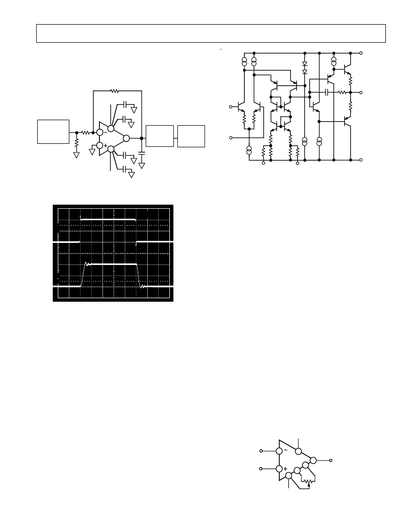
DRIVING CAPACIT IVE LOADS
T he internal compensation of the AD817, together with its high
output current drive, permit excellent large signal performance
while driving extremely high capacitive loads.
C
L
1000pF
R
IN
1k
+V
S
TEKTRONIX
P6201 FET
PROBE
HP
PULSE
GENERATOR
50
1k
V
OUT
0.01
μ
F
3.3
μ
F
–V
S
V
IN
TEKTRONIX
7A24
PREAMP
AD817
7
6
3
2
4
0.01
μ
F
3.3
μ
F
Figure 30a. Inverting Amplifier Driving a 1000 pF
Capacitive Load
10
90
100
0%
5V
500ns
5V
100pF
1000pF
Figure 30b. Inverting Amplifier Pulse Response While
Driving Capacitive Loads
T HE ORY OF OPE RAT ION
T he AD817 is a low cost, wide band, high performance opera-
tional amplifier which effectively drives heavy capacitive or resis-
tive loads. It also provides a constant slew rate, bandwidth and
settling time over its entire specified temperature range.
T he AD817 (Figure 31) consists of a degenerated NPN differ-
ential pair driving matched PNPs in a folded-cascode gain stage.
T he output buffer stage employs emitter followers in a class AB
amplifier which delivers the necessary current to the load while
maintaining low levels of distortion.
T he capacitor, C
F
, in the output stage mitigates the effect of
capacitive loads. At low frequencies, and with low capacitive
loads, the gain from the compensation node to the output is
very close to unity. In this case, C
F
is bootstrapped and does not
contribute to the overall compensation capacitance of the device.
As the capacitive load is increased, a pole is formed with the
output impedance of the output stage. T his reduces the gain,
and therefore, C
F
is incompletely bootstrapped. Effectively,
some fraction of C
F
contributes to the overall compensation
capacitance, reducing the unity gain bandwidth. As the load
capacitance is further increased, the bandwidth continues to fall,
maintaining the stability of the amplifier.
C
F
–IN
+IN
NULL 1
NULL 8
OUTPUT
+V
S
–V
S
Figure 31. Simplified Schematic
INPUT CONSIDE RAT IONS
An input protection resistor (R
IN
in Figure 22) is required in cir-
cuits where the input to the AD817 will be subjected to tran-
sient or continuous overload voltages exceeding the +6 V
maximum differential limit. T his resistor provides protection for
the input transistors by limiting their maximum base current.
For high performance circuits, it is recommended that a “bal-
ancing” resistor be used to reduce the offset errors caused by
bias current flowing through the input and feedback resistors.
T he balancing resistor equals the parallel combination of R
IN
and R
F
and thus provides a matched impedance at each input
terminal. T he offset voltage error will then be reduced by more
than an order of magnitude.
GROUNDING & BY PASSING
When designing high frequency circuits, some special precau-
tions are in order. Circuits must be built with short interconnect
leads. When wiring components, care should be taken to pro-
vide a low resistance, low inductance path to ground. Sockets
should be avoided, since their increased interlead capacitance
can degrade circuit bandwidth.
Feedback resistors should be of low enough value (<1 k
) to
assure that the time constant formed with the inherent stray
capacitance at the amplifier’s summing junction will not limit
performance. T his parasitic capacitance, along with the parallel
resistance of R
F
/R
IN
, form a pole in the loop transmission which
may result in peaking. A small capacitance (1 pF–5 pF) may be
used in parallel with the feedback resistor to neutralize this effect.
Power supply leads should be bypassed to ground as close as
possible to the amplifier pins. Ceramic disc capacitors of 0.1
μ
F
are recommended.
+V
S
10k
–V
S
AD817
7
3
2
4
8
6
1
V
OS
ADJUST
Figure 32. Offset Null Configuration
相關PDF資料 |
PDF描述 |
|---|---|
| AD8180-EB | 750 MHz, 3.8 mA 10 ns Switching Multiplexers |
| AD8180AN | 750 MHz, 3.8 mA 10 ns Switching Multiplexers |
| AD8180AR | 750 MHz, 3.8 mA 10 ns Switching Multiplexers |
| AD8180AR-REEL | 750 MHz, 3.8 mA 10 ns Switching Multiplexers |
| AD8180AR-REEL7 | 750 MHz, 3.8 mA 10 ns Switching Multiplexers |
相關代理商/技術參數(shù) |
參數(shù)描述 |
|---|---|
| AD8170 | 制造商:AD 制造商全稱:Analog Devices 功能描述:250 MHz, 10 ns Switching Multiplexers w/Amplifier |
| AD8170AN | 制造商:Analog Devices 功能描述:Analog Multiplexer Single 2:1 8-Pin PDIP Tube 制造商:Analog Devices 功能描述:IC MUX 2CH 250MHZ 8170 DIP8 |
| AD8170ANZ | 功能描述:IC MUX SWITCHING W/AMP 2:1 8DIP RoHS:是 類別:集成電路 (IC) >> 接口 - 專用 系列:- 特色產品:NXP - I2C Interface 標準包裝:1 系列:- 應用:2 通道 I²C 多路復用器 接口:I²C,SM 總線 電源電壓:2.3 V ~ 5.5 V 封裝/外殼:16-TSSOP(0.173",4.40mm 寬) 供應商設備封裝:16-TSSOP 包裝:剪切帶 (CT) 安裝類型:表面貼裝 產品目錄頁面:825 (CN2011-ZH PDF) 其它名稱:568-1854-1 |
| AD8170AR | 功能描述:IC MUX W/AMP BUFFERED 8-SOIC RoHS:否 類別:集成電路 (IC) >> 接口 - 專用 系列:- 特色產品:NXP - I2C Interface 標準包裝:1 系列:- 應用:2 通道 I²C 多路復用器 接口:I²C,SM 總線 電源電壓:2.3 V ~ 5.5 V 封裝/外殼:16-TSSOP(0.173",4.40mm 寬) 供應商設備封裝:16-TSSOP 包裝:剪切帶 (CT) 安裝類型:表面貼裝 產品目錄頁面:825 (CN2011-ZH PDF) 其它名稱:568-1854-1 |
| AD8170AR-REEL | 制造商:Analog Devices 功能描述:Analog Multiplexer Single 2:1 8-Pin SOIC N T/R 制造商:Rochester Electronics LLC 功能描述:SOIC 2:1 BUFFERED MULTIPLEXER - Tape and Reel |
發(fā)布緊急采購,3分鐘左右您將得到回復。