- 您現(xiàn)在的位置:買賣IC網(wǎng) > PDF目錄373940 > AD8189Z-EVALZ (Analog Devices, Inc.) 350 MHz Single-Supply (5 V) Triple 2:1 Multiplexers PDF資料下載
參數(shù)資料
| 型號(hào): | AD8189Z-EVALZ |
| 廠商: | Analog Devices, Inc. |
| 英文描述: | 350 MHz Single-Supply (5 V) Triple 2:1 Multiplexers |
| 中文描述: | 350兆赫單電源(5V)的三重2:1多路復(fù)用器 |
| 文件頁數(shù): | 15/24頁 |
| 文件大小: | 725K |
| 代理商: | AD8189Z-EVALZ |
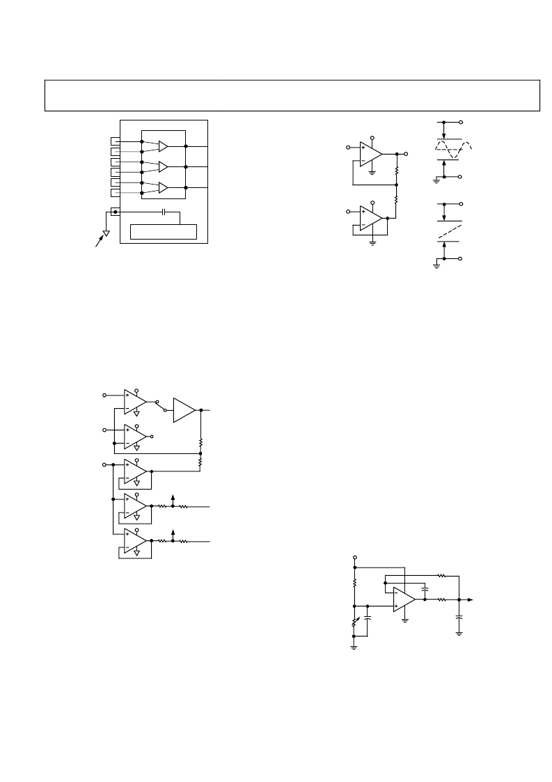
AD8188/AD8189
Rev. 0 | Page 15 of 24
IN0A
IN0B
IN1B
IN1A
IN2A
IN2B
OUT0
OUT1
OUT2
AD8188
MUX SYSTEM
“C_BYPASS”
V
REF
INTERNAL CAP
BIAS REFERENCE
DIRECT CONNECTION TO ANY “QUIET” AC GROUND
(FOR EXAMPLE, GND, V
CC
, AND V
EE
).
0
Figure 45. V
REF
Pin Connection for AD8188 (Differs from AD8189)
The AD8189
The AD8189 uses on-chip feedback resistors to realize the gain-
of-two function. To provide low crosstalk and a high output
impedance when disabled, each set of 500 Ω feedback resistors
is terminated by a dedicated reference buffer. A reference buffer
is a high speed op amp configured as a unity-gain follower. The
three reference buffers, one for each channel, share a single,
high impedance input, the V
REF
pin (see Figure 46). V
REF
input
bias current is typically less than 2 μA.
OUT1
OUT0
OUT2
A0
B0
V
REF
5V
5V
5V
GBUF 0
5V
GBUF 1
5V
GBUF 2
500
500
500
500
500
500
VF-2
VF-1
1×
VFO
0
Figure 46. Conceptual Diagram of a Single Multiplexer Channel, G = 2
This configuration has a few implications for single-supply
operation:
On the AD8189, V
REF
cannot be tied to the most negative
analog supply, V
EE
. The limits on reference voltage are (see
Figure 47):
V
EE
+ 1.3 V <
V
REF
×
V
CC
1.6 V
1.3 V <
V
REF
,
3.4 V on 0 V/5 V supplies
A0
V
REF
5V
5V
OUT0
5V
V
O_MAX
= 3.7V
V
O_MIN
= 1.3V
V
O_MIN
= 1.3V
V
O_MAX
= 3.4V
5V
1.3V
1.3V
1.3V
1.6V
GND
GND
V
OUT
V
REF
0
Figure 47. Output Compliance of Main Amplifier Channel and Ground Buffer
The signal at the V
REF
pin appears at each output.
Therefore, V
REF
should be tied to a well bypassed, low
impedance source. Using superposition, it is shown that
V
OUT
= 2 ×
V
IN
V
REF
To maximize the output dynamic range, the reference
voltage should be chosen with care. For example, consider
amplifying a 700 mV video signal with a sync pulse
300 mV below black level. If the user decides to set V
REF
at
black level to preferentially run video signals on the faster
NPN transistor path, the AD8189 allows a reference
voltage as low as 1.3 V + 300 mV = 1.6 V. If the AD8189 is
used, the sync pulse is amplified to 600 mV. Therefore, the
lower limit on V
REF
becomes 1.3 V + 600 mV = 1.9 V. For
routing RGB video, an advantageous configuration is to
employ +3 V and 2 V supplies, in which case V
REF
can be
tied to ground.
If system considerations prevent running the multiplexer on
split supplies, a false ground reference should be employed. A
low impedance reference can be synthesized with a second
operational amplifier. Alternately, a well bypassed resistor
divider can be used. Refer to the Applications section for
further explanation and more examples.
V
REF
0.022μF
5V
GND
OP21
100k
10k
100
FROM 1992 ADI AMPLIFIER
APPLICATIONS GUIDE
1μF
1μF
0
Figure 48. Synthesis of a False Ground Reference
相關(guān)PDF資料 |
PDF描述 |
|---|---|
| AD8188 | 350 MHz Single-Supply (5 V) Triple 2:1 Multiplexers |
| AD8188ARUZ | 350 MHz Single-Supply (5 V) Triple 2:1 Multiplexers |
| AD8188ARUZ-R7 | 350 MHz Single-Supply (5 V) Triple 2:1 Multiplexers |
| AD818AR-REEL | Low Cost, Low Power Video Op Amp |
| AD818AR-REEL7 | Low Cost, Low Power Video Op Amp |
相關(guān)代理商/技術(shù)參數(shù) |
參數(shù)描述 |
|---|---|
| AD818AN | 制造商:Analog Devices 功能描述:OP Amp Single Volt Fdbk 制造商:Analog Devices 功能描述:IC AMP VIDEO LOW POWER DIP8 818 |
| AD818AN | 制造商:Analog Devices 功能描述:SEMICONDUCTORSLINEAR |
| AD818ANZ | 功能描述:IC VIDEO OPAMP 130MHZ LP 8-DIP RoHS:是 類別:集成電路 (IC) >> 線性 - 放大器 - 視頻放大器和頻緩沖器 系列:- 產(chǎn)品培訓(xùn)模塊:Lead (SnPb) Finish for COTS Obsolescence Mitigation Program 標(biāo)準(zhǔn)包裝:50 系列:- 應(yīng)用:TFT-LCD 面板:VCOM 驅(qū)動(dòng)器 輸出類型:滿擺幅 電路數(shù):1 -3db帶寬:35MHz 轉(zhuǎn)換速率:40 V/µs 電流 - 電源:3.7mA 電流 - 輸出 / 通道:1.3A 電壓 - 電源,單路/雙路(±):9 V ~ 20 V,±4.5 V ~ 10 V 安裝類型:表面貼裝 封裝/外殼:8-TSSOP,8-MSOP(0.118",3.00mm 寬)裸露焊盤 供應(yīng)商設(shè)備封裝:8-uMax-EP 包裝:管件 |
| AD818AR | 功能描述:IC VIDEO OPAMP 130MHZ LP 8-SOIC RoHS:否 類別:集成電路 (IC) >> 線性 - 放大器 - 視頻放大器和頻緩沖器 系列:- 標(biāo)準(zhǔn)包裝:1,000 系列:- 應(yīng)用:驅(qū)動(dòng)器 輸出類型:差分 電路數(shù):3 -3db帶寬:350MHz 轉(zhuǎn)換速率:1000 V/µs 電流 - 電源:14.5mA 電流 - 輸出 / 通道:60mA 電壓 - 電源,單路/雙路(±):5 V ~ 12 V,±2.5 V ~ 6 V 安裝類型:表面貼裝 封裝/外殼:20-VFQFN 裸露焊盤 供應(yīng)商設(shè)備封裝:20-QFN 裸露焊盤(4x4) 包裝:帶卷 (TR) |
| AD818AR-EBZ | 功能描述:BOARD EVAL FOR AD818AR RoHS:是 類別:編程器,開發(fā)系統(tǒng) >> 評(píng)估演示板和套件 系列:* 標(biāo)準(zhǔn)包裝:1 系列:- 主要目的:電信,線路接口單元(LIU) 嵌入式:- 已用 IC / 零件:IDT82V2081 主要屬性:T1/J1/E1 LIU 次要屬性:- 已供物品:板,電源,線纜,CD 其它名稱:82EBV2081 |
發(fā)布緊急采購,3分鐘左右您將得到回復(fù)。