- 您現在的位置:買賣IC網 > PDF目錄373942 > AD826AR-REEL7 (ANALOG DEVICES INC) High-Speed, Low-Power Dual Operational Amplifier PDF資料下載
參數資料
| 型號: | AD826AR-REEL7 |
| 廠商: | ANALOG DEVICES INC |
| 元件分類: | 運動控制電子 |
| 英文描述: | High-Speed, Low-Power Dual Operational Amplifier |
| 中文描述: | DUAL OP-AMP, 3000 uV OFFSET-MAX, 20 MHz BAND WIDTH, PDSO8 |
| 封裝: | PLASTIC, MS-012AA, SOIC-8 |
| 文件頁數: | 10/14頁 |
| 文件大小: | 231K |
| 代理商: | AD826AR-REEL7 |
REV. B
AD826
–10–
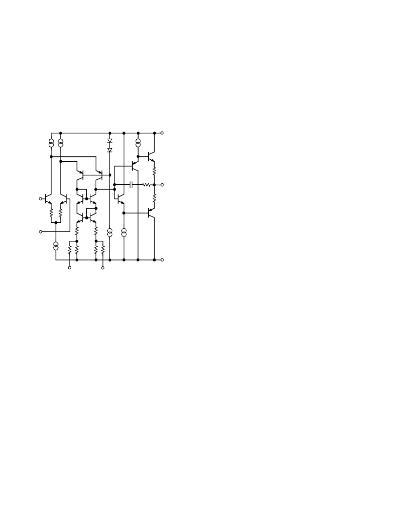
THEORY OF OPERATION
The AD826 is a low cost, wide band, high performance dual
operational amplifier which can drive heavy capacitive and
resistive loads. It also achieves a constant slew rate, bandwidth
and settling time over its entire specified temperature range.
The AD826 (Figure 35) consists of a degenerated NPN differen-
tial pair driving matched PNPs in a folded-cascode gain stage.
The output buffer stage employs emitter followers in a class AB
amplifier which delivers the necessary current to the load while
maintaining low levels of distortion.
C
F
–
IN
+IN
NULL 1
NULL 8
OUTPUT
+V
S
–
V
S
Figure 35. Simplified Schematic
The capacitor, C
F
, in the output stage mitigates the effect of
capacitive loads. With low capacitive loads, the gain from the
compensation node to the output is very close to unity. In this
case, C
F
is bootstrapped and does not contribute to the overall
compensation capacitance of the device. As the capacitive load
is increased, a pole is formed with the output impedance of the
output stage. This reduces the gain, and therefore, C
F
is
incompletely bootstrapped. Effectively, some fraction of C
F
contributes to the overall compensation capacitance, reducing
the unity gain bandwidth. As the load capacitance is further
increased, the bandwidth continues to fall, maintaining the
stability of the amplifier.
INPUT CONSIDERATIONS
An input protection resistor (R
IN
in Figure 25) is required in
circuits where the input to the AD826 will be subjected to
transient or continuous overload voltages exceeding the
±
6 V
maximum differential limit. This resistor provides protection for
the input transistors by limiting their maximum base current.
For high performance circuits, it is recommended that a “bal-
ancing” resistor be used to reduce the offset errors caused by
bias current flowing through the input and feedback resistors.
The balancing resistor equals the parallel combination of R
IN
and R
F
and thus provides a matched impedance at each input
terminal. The offset voltage error will then be reduced by more
than an order of magnitude.
APPLYING THE AD826
The AD826 is a breakthrough dual amp that delivers precision
and speed at low cost with low power consumption. The AD826
offers excellent static and dynamic matching characteristics,
combined with the ability to drive heavy resistive and capacitive
loads.
As with all high frequency circuits, care should be taken to main-
tain overall device performance as well as their matching. The
following items are presented as general design considerations.
Circuit Board Layout
Input and output runs should be laid out so as to physically
isolate them from remaining runs. In addition, the feedback
resistor of each amplifier should be placed away from the
feedback resistor of the other amplifier, since this greatly
reduces inter-amp coupling.
Choosing Feedback and Gain Resistors
In order to prevent the stray capacitance present at each amplifier’s
summing junction from limiting its performance, the feedback
resistors should be
≤
1 k
. Since the summing junction capaci-
tance may cause peaking, a small capacitor (1 pF–5 pF) may
be paralleled with R
F
to neutralize this effect. Finally, sockets
should be avoided, because of their tendency to increase interlead
capacitance.
Power Supply Bypassing
Proper power supply decoupling is critical to preserve the
integrity of high frequency signals. In carefully laid out designs,
decoupling capacitors should be placed in close proximity to the
supply pins, while their lead lengths should be kept to a mini-
mum. These measures greatly reduce undesired inductive effects
on the amplifier’s response.
Though two 0.1
μ
F capacitors will typically be effective in
decoupling the supplies, several capacitors of different values
can be paralleled to cover a wider frequency range.
相關PDF資料 |
PDF描述 |
|---|---|
| AD827JR-REEL | High Speed, Low Power Dual Op Amp |
| AD827 | High Speed, Low Power Dual Op Amp |
| AD827AQ | High Speed, Low Power Dual Op Amp |
| AD827JN | High Speed, Low Power Dual Op Amp |
| AD827JR | High Speed, Low Power Dual Op Amp |
相關代理商/技術參數 |
參數描述 |
|---|---|
| AD826ARZ | 功能描述:IC OPAMP VF 50MHZ DUAL LP 8SOIC RoHS:是 類別:集成電路 (IC) >> Linear - Amplifiers - Instrumentation 系列:- 標準包裝:2,500 系列:- 放大器類型:通用 電路數:4 輸出類型:- 轉換速率:0.6 V/µs 增益帶寬積:1MHz -3db帶寬:- 電流 - 輸入偏壓:45nA 電壓 - 輸入偏移:2000µV 電流 - 電源:1.4mA 電流 - 輸出 / 通道:40mA 電壓 - 電源,單路/雙路(±):3 V ~ 32 V,±1.5 V ~ 16 V 工作溫度:0°C ~ 70°C 安裝類型:表面貼裝 封裝/外殼:14-TSSOP(0.173",4.40mm 寬) 供應商設備封裝:14-TSSOP 包裝:帶卷 (TR) 其它名稱:LM324ADTBR2G-NDLM324ADTBR2GOSTR |
| AD826ARZ-REEL | 功能描述:IC OPAMP VF 50MHZ DUAL LP 8SOIC RoHS:是 類別:集成電路 (IC) >> Linear - Amplifiers - Instrumentation 系列:- 標準包裝:100 系列:- 放大器類型:通用 電路數:1 輸出類型:- 轉換速率:0.2 V/µs 增益帶寬積:- -3db帶寬:- 電流 - 輸入偏壓:100pA 電壓 - 輸入偏移:30µV 電流 - 電源:380µA 電流 - 輸出 / 通道:- 電壓 - 電源,單路/雙路(±):±2 V ~ 18 V 工作溫度:0°C ~ 70°C 安裝類型:表面貼裝 封裝/外殼:8-SOIC(0.154",3.90mm 寬) 供應商設備封裝:8-SO 包裝:管件 |
| AD826ARZ-REEL7 | 功能描述:IC OPAMP VF 50MHZ DUAL LP 8SOIC RoHS:是 類別:集成電路 (IC) >> Linear - Amplifiers - Instrumentation 系列:- 標準包裝:100 系列:- 放大器類型:通用 電路數:1 輸出類型:- 轉換速率:0.2 V/µs 增益帶寬積:- -3db帶寬:- 電流 - 輸入偏壓:100pA 電壓 - 輸入偏移:30µV 電流 - 電源:380µA 電流 - 輸出 / 通道:- 電壓 - 電源,單路/雙路(±):±2 V ~ 18 V 工作溫度:0°C ~ 70°C 安裝類型:表面貼裝 封裝/外殼:8-SOIC(0.154",3.90mm 寬) 供應商設備封裝:8-SO 包裝:管件 |
| AD827 | 制造商:AD 制造商全稱:Analog Devices 功能描述:High Speed, Low Power Dual Op Amp |
| AD827_02 | 制造商:AD 制造商全稱:Analog Devices 功能描述:High Speed, Low Power Dual Op Amp |
發布緊急采購,3分鐘左右您將得到回復。