- 您現在的位置:買賣IC網 > PDF目錄373942 > AD8304ARU-REEL (ANALOG DEVICES INC) 160 dB Range (100 pA -10 mA) Logarithmic Converter PDF資料下載
參數資料
| 型號: | AD8304ARU-REEL |
| 廠商: | ANALOG DEVICES INC |
| 元件分類: | 運動控制電子 |
| 英文描述: | 160 dB Range (100 pA -10 mA) Logarithmic Converter |
| 中文描述: | LOG OR ANTILOG AMPLIFIER, 10 MHz BAND WIDTH, PDSO14 |
| 封裝: | MO-153AB-1, TSSOP-14 |
| 文件頁數: | 12/20頁 |
| 文件大小: | 4286K |
| 代理商: | AD8304ARU-REEL |
REV. A
–12–
AD8304
6
3
4
PDB
BIAS
VREF
10
2
12
VPDB
VSUM
INPT
VSUM
5
1
VNEG
~10k
ACOM
14
VPS2
PWDN
VPS1
VREF
7
VLOG
8
BFIN
9
BFNG
TEMPERATURE
COMPENSATION
5k
11
VOUT
0.5V
I
PD
NC
R1
750
10nF
C1
1nF
13
RA
V
P
V
OUT
NC = NO CONNECT
RB
RC
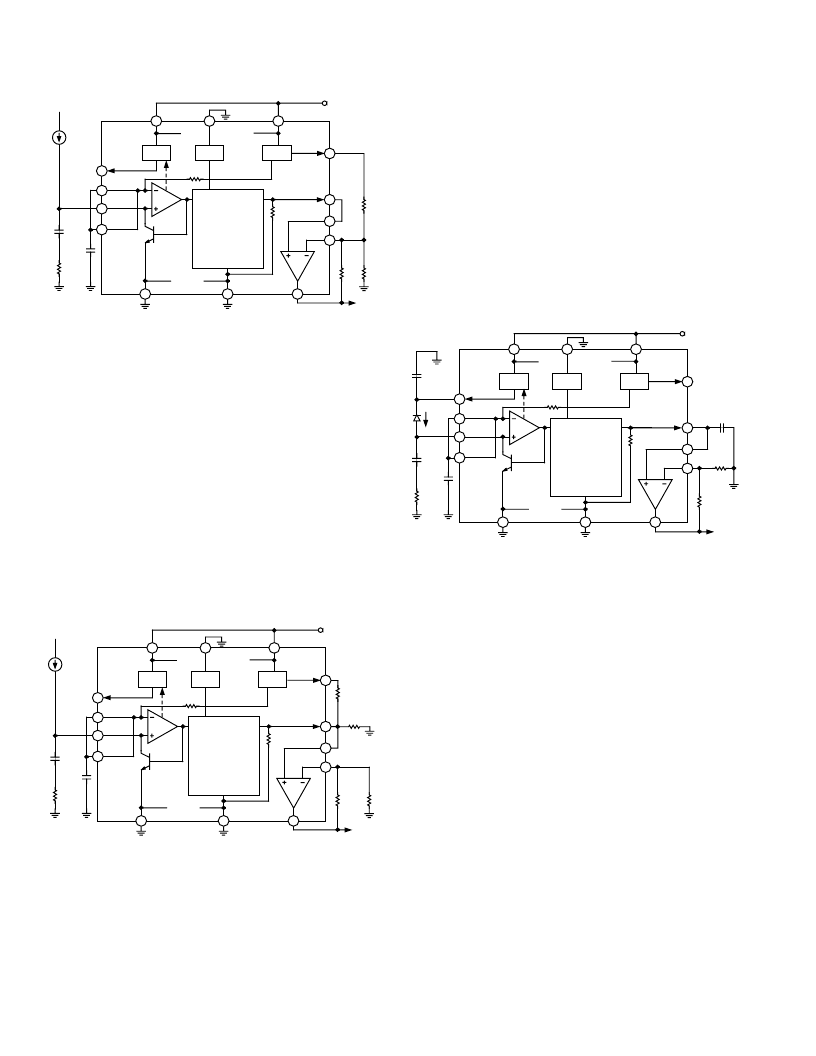
Figure 5. Method for Raising the Intercept
Low Supply Slope and Intercept Adjustment
When using the device with a positive supply less than 4 V, it is
necessary to reduce the slope and intercept at the VLOG Pin in
order to preserve good log conformance over the entire 160 dB
operating range. The voltage at the VLOG Pin is generated by
an internal current source with an output current of 40
μ
A/decade
feeding the internal laser-trimmed output resistance of 5 k
. When
the voltage at the VLOG Pin exceeds V
P
–
2.3 V, the current
source ceases to respond linearly to logarithmic increases in current.
This headroom issue can be avoided by reducing the logarithmic
slope and intercept at the VLOG Pin. This is accomplished by
connecting an external resistor R
S
from the VLOG Pin to ground
in combination with an intercept lowering resistor R
Z
. The values
shown in Figure 6 illustrate a good solution for a 3.0 V positive
supply. The resulting logarithmic slope measured at VLOG is
62.5 mV/decade with a new intercept of 57 fA. The original
logarithmic slope of 200 mV/decade can be recovered using voltage
gain on the internal buffer amplifier.
6
3
4
PDB
BIAS
VREF
10
2
12
VPDB
VSUM
INPT
VSUM
5
1
VNEG
~10k
ACOM
14
VPS2
PWDN
VPS1
VREF
7
VLOG
8
BFIN
9
BFNG
TEMPERATURE
COMPENSATION
5k
11
VOUT
0.5V
I
PD
NC
R1
750
10nF
C1
1nF
13
RA
4.98k
V
P
V
OUT
NC = NO CONNECT
RB
2.26k
RS
2.67k
RZ
15.4k
62.5mV/DEC
Figure 6. Recommended Low Supply Application Circuit
Using the Adaptive Bias
For most photodiode applications, the placement of the anode
somewhat above ground is acceptable, as long as the positive
bias on the cathode is adequate to support the peak current for a
particular diode, limited mainly by its series resistance. To address
this matter, the AD8304 provides for the diode a bias that varies
linearly with the current. This voltage appears at Pin VPDB, and
varies from 0.6 V (reverse-biasing the diode by 0.1 V) for I
PD
=
100 pA and rises to 2.6 V (for a diode bias of 1 V) at I
PD
= 10 mA.
This results in a constant internal junction bias of 0.1 V when the
series resistance of the photodiode is 200
. For optical power
measurements over a wide dynamic range the adaptive biasing
function will be valuable in minimizing dark current while pre-
venting the loss of photodiode bias at high currents. Use of the
adaptive bias feature is shown in Figure 7.
6
3
4
PDB
BIAS
VREF
10
2
12
VPDB
VSUM
INPT
VSUM
5
1
VNEG
~10k
ACOM
14
VPS2
PWDN
VPS1
VREF
7
VLOG
8
BFIN
9
BFNG
TEMPERATURE
COMPENSATION
5k
11
VOUT
0.5V
I
PD
CPB
R1
750
10nF
C1
1nF
13
RA
RB
CFILT
V
P
V
OUT
Figure 7. Using the Adaptive Biasing
Capacitor CPB, between the photodiode cathode at Pin VPDB
and ground, is included to lower the impedance at this node and
thereby improve the high frequency accuracy at those current
levels where the AD8304 bandwidth is high. It also ensures an
HF path for any high frequency modulation on the optical signal
which might not otherwise be accurately averaged. It will not be
necessary in all cases, and experimentation may be required to find
an optimum value.
Changing the Voltage at the Summing Node
The default value of VSUM is determined by using a quarter of
VREF (2 V). This may be altered by applying an independent volt-
age source to VSUM, or by adding an external resistive divider
from VREF
to VSUM. This network will operate in parallel with
the internal divider (40 k
and 13.3 k
), and the choice of external
resistors should take this into account. In practice, the total
resistance of the added string may be as low as 10 k
(consuming
400
μ
A from VREF). Low values of VSUM and thus V
CE
(see
Figure 13) are not advised when large values of I
PD
are expected.
Implementing Low-Pass Filters
Noise, leading to uncertainty in an observed value, is inherent to
all measurement systems. Translinear log amps exhibit significant
amounts of noise for reasons stated above, and are more trouble-
some at low current levels. The standard way of addressing this
problem is to average the measurement over an appropriate time
interval. This can be achieved in the digital domain, in post-ADC
DSP, or in analog form using a variety of low-pass structures.
相關PDF資料 |
PDF描述 |
|---|---|
| AD8304 | 160 dB Range (100 pA -10 mA) Logarithmic Converter |
| AD8304-EVAL | 160 dB Range (100 pA -10 mA) Logarithmic Converter |
| AD8304ARU | 160 dB Range (100 pA -10 mA) Logarithmic Converter |
| AD8304ARU-REEL7 | 160 dB Range (100 pA -10 mA) Logarithmic Converter |
| AD8305 | 100 dB Range (10 nA to 1 mA) Logarithmic Converter |
相關代理商/技術參數 |
參數描述 |
|---|---|
| AD8304ARU-REEL7 | 功能描述:IC LOGARITHMIC CONV 14-TSSOP T/R RoHS:否 類別:集成電路 (IC) >> 線性 - 放大器 - 專用 系列:- 產品培訓模塊:Lead (SnPb) Finish for COTS Obsolescence Mitigation Program 標準包裝:60 系列:- 類型:可變增益放大器 應用:CATV 安裝類型:表面貼裝 封裝/外殼:20-WQFN 裸露焊盤 供應商設備封裝:20-TQFN-EP(5x5) 包裝:托盤 |
| AD8304ARUZ | 功能描述:IC LOGARITHM CONV 160DB 14-TSSOP RoHS:是 類別:集成電路 (IC) >> 線性 - 放大器 - 專用 系列:- 產品培訓模塊:Lead (SnPb) Finish for COTS Obsolescence Mitigation Program 標準包裝:60 系列:- 類型:可變增益放大器 應用:CATV 安裝類型:表面貼裝 封裝/外殼:20-WQFN 裸露焊盤 供應商設備封裝:20-TQFN-EP(5x5) 包裝:托盤 |
| AD8304ARUZ | 制造商:Analog Devices 功能描述:Logarithmic Amplifier IC |
| AD8304ARUZ-RL7 | 功能描述:IC LOGARITHM CONV 160DB 14-TSSOP RoHS:是 類別:集成電路 (IC) >> 線性 - 放大器 - 專用 系列:- 產品培訓模塊:Lead (SnPb) Finish for COTS Obsolescence Mitigation Program 標準包裝:60 系列:- 類型:可變增益放大器 應用:CATV 安裝類型:表面貼裝 封裝/外殼:20-WQFN 裸露焊盤 供應商設備封裝:20-TQFN-EP(5x5) 包裝:托盤 |
| AD8304-EVAL | 制造商:Analog Devices 功能描述:LTSSOP 160DB-RANGE LOGARITHMIC CONVERTER - Bulk |
發布緊急采購,3分鐘左右您將得到回復。