- 您現在的位置:買賣IC網 > PDF目錄373942 > AD8305ACP-REEL7 (ANALOG DEVICES INC) 100 dB Range (10 nA to 1 mA) Logarithmic Converter PDF資料下載
參數資料
| 型號: | AD8305ACP-REEL7 |
| 廠商: | ANALOG DEVICES INC |
| 元件分類: | 運動控制電子 |
| 英文描述: | 100 dB Range (10 nA to 1 mA) Logarithmic Converter |
| 中文描述: | LOG OR ANTILOG AMPLIFIER, QCC16 |
| 封裝: | 3 X 3 MM, MINIATURE, MO-220-VEED-2, LFCSP-16 |
| 文件頁數: | 9/20頁 |
| 文件大小: | 1301K |
| 代理商: | AD8305ACP-REEL7 |
REV. A
AD8305
–9–
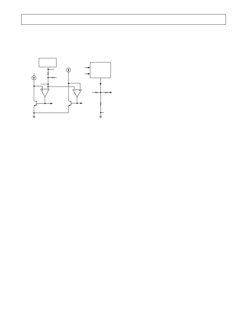
GENERAL STRUCTURE
The AD8305 addresses a wide variety of interfacing conditions
to meet the needs of fiber optic supervisory systems, and will
also be useful in many nonoptical applications. These notes
explain the structure of this unique style of translinear log amp.
Figure 1 is a simplified schematic showing the key elements.
TEMPERATURE
COMPENSATION
(SUBTRACT AND
DIVIDE BY T K
BIAS
GENERATOR
VLOG
COMM
VNEG (NORMALLY GROUNDED)
VSUM
INPT
0.5V
80k
0.5V
0.5V
V
BE2
V
BE2
V
BE1
V
BE1
44 A/dec
I
REF
I
PD
6.69k
Q2
Q1
PHOTODIODE
INPUT CURRENT
COMM
20k
451
VREF
VRDZ
IREF
14.2k
2.5V
Figure 1. Simplified Schematic
The photodiode current I
PD
is received at Pin INPT. The
voltage at this node is essentially equal to those on the two
adjacent guard pins, VSUM and IREF, due to the low offset
voltage of the JFET op amp. Transistor Q1 converts the input
current I
PD
to a corresponding logarithmic voltage, as shown in
Equation 1. A finite positive value of V
SUM
is needed to bias
the collector of Q1 for the usual case of a single-supply voltage.
This is internally set to 0.5 V, that is, one fifth of the reference
voltage of 2.5 V appearing on Pin VREF. The resistance at the
VSUM pin is nominally 16 k
W
; this voltage is not intended as
a general bias source.
The AD8305 also supports the use of an optional negative supply
voltage, V
N
, at Pin VNEG. When V
N
is –0.5 V or more negative,
VSUM may be connected to ground; thus INPT and IREF
assume this potential. This allows operation as a voltage-input
logarithmic converter by the inclusion of a series resistor at either
or both inputs. Note that the resistor setting I
REF
will need to be
adjusted to maintain the intercept value. It should also be noted
that the collector-emitter voltages of Q1 and Q2 are now the full
V
N
, and effects due to self-heating will cause errors at large
input currents.
The input dependent V
BE1
of Q1 is compared with the reference
V
BE2
of a second transistor, Q2, operating at I
REF
. This is gener-
ated externally, to a recommended value of 10
A. However,
other values over a several-decade range can be used with a
slight degradation in law conformance (TPC 1).
Theory
The base-emitter voltage of a BJT (bipolar junction transistor)
can be expressed by Equation 1, which immediately shows its
basic logarithmic nature:
V
where
I
is its collector current,
I
S
is a scaling current, typically
only 10
C
A, and
kT
/
q
is the thermal voltage, proportional to
absolute temperature (PTAT) and is 25.85 mV at 300 K. The
current,
I
S
,
is never precisely defined and exhibits an even stron-
ger temperature dependence, varying by a factor of roughly a
kT q
I
I
BE
C
S
=
(
)
/
/
In
(1)
billion between –35
∞
C and +85
∞
C. Thus, to make use of the
BJT as an accurate logarithmic element, both of these tempera-
ture dependencies must be eliminated.
The difference between the base-emitter voltages of a matched pair
of BJTs, one operating at the photodiode current
I
PD
and the second
operating at a reference current
I
REF
, can be written as:
V
V
kT q
I I
kT q
mV
.
log
=
59 5
10
The uncertain and temperature dependent saturation current
I
S
,
which appears in Equation 1, has thus been eliminated. To
eliminate the temperature variation of
kT
/
q
, this difference voltage
is processed by what is essentially an analog divider. Effectively, it
puts a variable under Equation 2. The output of this process,
which also involves a conversion from voltage-mode to current-
mode, is an intermediate, temperature-corrected current:
I
where
I
Y
is an accurate, temperature-stable scaling current that
determines the slope of the function (the change in current per
decade). For the AD8305,
I
Y
is 44
m
A, resulting in a temperature-
independent slope of 44
m
A/decade, for all values of
I
PD
and
I
REF
.
This current is subsequently converted back to a voltage-mode
output, V
LOG
, scaled 200 mV/decade.
It is apparent that this output should be zero for
I
PD
= I
REF
, and
would need to swing negative for smaller values of input current.
To avoid this, I
REF
would need to be as small as the smallest
value of
I
PD
. However, it is impractical to use such a small refer-
ence current as 1 nA. Accordingly, an offset voltage is added to
V
LOG
to shift it upward by 0.8 V when Pin VRDZ is directly
connected to VREF. This has the effect of moving the intercept
to the left by four decades, from 10
m
A to 1 nA:
I
where
I
INTC
is the operational value of the intercept current. To
disable this offset, Pin VRDZ should be grounded, then the
intercept
I
INTC
is simply I
REF
. Since values of
I
PD
<
I
INTC
result in
a negative V
LOG
, a negative supply of sufficient value is required
to accommodate this situation (discussed later).
The voltage
V
LOG
is generated by applying
I
LOG
to an internal
resistance of 4.55 k
W
, formed by the parallel combination of a
6.69 k
W
resistor to ground and the 14.2 k
W
resistor to the VRDZ
pin. When the VLOG pin is unloaded and the intercept reposi-
tioning is disabled by grounding VRDZ, the output current
I
LOG
generates a voltage at the VLOG pin of:
V
I
A
=
=
10
log
/
I
PD
where
V
Y
= 200 mV/decade, or 10 mV/dB. Note that any resistive
loading on VLOG will lower this slope and also result in an
overall scaling uncertainty due to the variability of the on-chip
resistors. Consequently, this practice is not recommended.
V
LOG
may also swing below ground when dual supplies (V
P
and
V
N
) are used. When V
N
= –0.5 V or larger, the input pins INPT
and IREF may now be positioned at ground level by simply
grounding VSUM.
kT q
I
I
PD
I
I
I
I
T
(
K
S
REF
S
PD
/
REF
)
REF
BE1
BE2
–
/
( )
/
/ log
–
/
/
/
=
(
)
(
)
=
(
(
=
)
In
In
In
10
300
10
(2)
I
I
I
LOG
Y
PD
REF
=
(
)
log
/
10
(3)
I
I
I
LOG
Y
PD
INTC
=
(
)
log
/
10
(4)
I
V
I
LOG
LOG
44
REF
Y
REF
=
¥
¥
¥
)
(
)
(
4 55
4 55
.
10
.
k
k
log
/
W
W
m
I
PD
(5)
相關PDF資料 |
PDF描述 |
|---|---|
| AD8306 | 5 MHz-400 MHz 100 dB High Precision Limiting-Logarithmic Amplifier |
| AD8306-EVAL | 5 MHz-400 MHz 100 dB High Precision Limiting-Logarithmic Amplifier |
| AD8306ACHIPS | 5 MHz-400 MHz 100 dB High Precision Limiting-Logarithmic Amplifier |
| AD8306AR | 5 MHz-400 MHz 100 dB High Precision Limiting-Logarithmic Amplifier |
| AD8306AR-REEL | 5 MHz-400 MHz 100 dB High Precision Limiting-Logarithmic Amplifier |
相關代理商/技術參數 |
參數描述 |
|---|---|
| AD8305ACPZ | 制造商:AD 制造商全稱:Analog Devices 功能描述:100 dB Range (10 nA to 1 mA) ogarithmic Converter |
| AD8305ACPZ-R2 | 功能描述:IC AMP LOG CONV 100DB 16-LFCSP RoHS:是 類別:集成電路 (IC) >> 線性 - 放大器 - 專用 系列:- 產品培訓模塊:Lead (SnPb) Finish for COTS Obsolescence Mitigation Program 標準包裝:60 系列:- 類型:可變增益放大器 應用:CATV 安裝類型:表面貼裝 封裝/外殼:20-WQFN 裸露焊盤 供應商設備封裝:20-TQFN-EP(5x5) 包裝:托盤 |
| AD8305ACPZ-RL7 | 功能描述:IC LOGARITH CONV 100DB 16-LFCSP RoHS:是 類別:集成電路 (IC) >> 線性 - 放大器 - 專用 系列:- 產品培訓模塊:Lead (SnPb) Finish for COTS Obsolescence Mitigation Program 標準包裝:60 系列:- 類型:可變增益放大器 應用:CATV 安裝類型:表面貼裝 封裝/外殼:20-WQFN 裸露焊盤 供應商設備封裝:20-TQFN-EP(5x5) 包裝:托盤 |
| AD8305BRU | 制造商:Analog Devices 功能描述:- Bulk |
| AD8305-EVAL | 制造商:Analog Devices 功能描述:Evaluation Board For IC Log Amp Single 12V 制造商:Analog Devices 功能描述:AD8305 EVALUATION BOARD - Bulk |
發布緊急采購,3分鐘左右您將得到回復。