- 您現(xiàn)在的位置:買賣IC網(wǎng) > PDF目錄373942 > AD8309ARU-REEL7 (ANALOG DEVICES INC) 5 MHz.500 MHz 100 dB Demodulating Logarithmic Amplifier with Limiter Output PDF資料下載
參數(shù)資料
| 型號(hào): | AD8309ARU-REEL7 |
| 廠商: | ANALOG DEVICES INC |
| 元件分類: | 運(yùn)動(dòng)控制電子 |
| 英文描述: | 5 MHz.500 MHz 100 dB Demodulating Logarithmic Amplifier with Limiter Output |
| 中文描述: | LOG OR ANTILOG AMPLIFIER, 495 MHz BAND WIDTH, PDSO16 |
| 封裝: | TSSOP-16 |
| 文件頁(yè)數(shù): | 8/20頁(yè) |
| 文件大小: | 311K |
| 代理商: | AD8309ARU-REEL7 |
第1頁(yè)第2頁(yè)第3頁(yè)第4頁(yè)第5頁(yè)第6頁(yè)第7頁(yè)當(dāng)前第8頁(yè)第9頁(yè)第10頁(yè)第11頁(yè)第12頁(yè)第13頁(yè)第14頁(yè)第15頁(yè)第16頁(yè)第17頁(yè)第18頁(yè)第19頁(yè)第20頁(yè)
REV. B
AD8309
–8–
As a consequence of this high gain, even very small amounts of
thermal noise at the input of a log amp will cause a finite output
for zero input, resulting in the response line curving away from
the ideal (Figure 19) at small inputs, toward a fixed baseline.
This can either be above or below the intercept, depending on
the design. Note that the value specified for this intercept is
invariably an
extrapolated
one: the RSSI output voltage will never
attain a value of exactly zero in a single supply implementation.
Voltage (dBV) and Power (dBm) Response
While Equation 1 is fundamentally correct, a simpler formula is
appropriate for specifying the RSSI calibration attributes of a
log amp like the AD8309, which
demodulates
an RF input. The
usual measure is input power:
V
OUT
=
V
SLOPE
(
P
IN
–
P
0
)
V
OUT
is the demodulated and filtered RSSI output,
V
SLOPE
is the
logarithmic slope, expressed in volts/dB,
P
IN
is the input power,
expressed in decibels relative to some reference power level and
P
0
is the logarithmic intercept, expressed in decibels relative to
the same reference level.
The most widely used convention in RF systems is to specify
power in decibels above 1 mW in 50
, written dBm. (However,
that the quantity [P
IN
– P
0
] is simply dB). The logarithmic
function disappears from this formula because the conversion
has already been implicitly performed in stating the input in
decibels.
Specification of log amp input level in terms of power is strictly
a concession to popular convention: they do
not
respond to
power
(tacitly “power absorbed at the input”), but to the input
voltage
. In this connection, note that the input impedance of the
AD8309 is much higher that 50
, allowing the use of an im-
pedance transformer at the input to raise the sensitivity, by up
to 13 dB.
The use of dBV, defined as
decibels with respect to a 1 V rms sine
amplitude
, is more precise, although this is still not unambiguous
complete as a general
metric, because waveform is also involved
in the response of a log amp, which, for a complex input (such
as a CDMA signal) will not follow the rms value exactly. Since
most users specify
RF signals in terms of power—more specifi-
cally, in dBm/50
—we use both dBV and dBm in specifying
the performance of the AD8309, showing equivalent dBm levels
for the special case of a 50
environment.
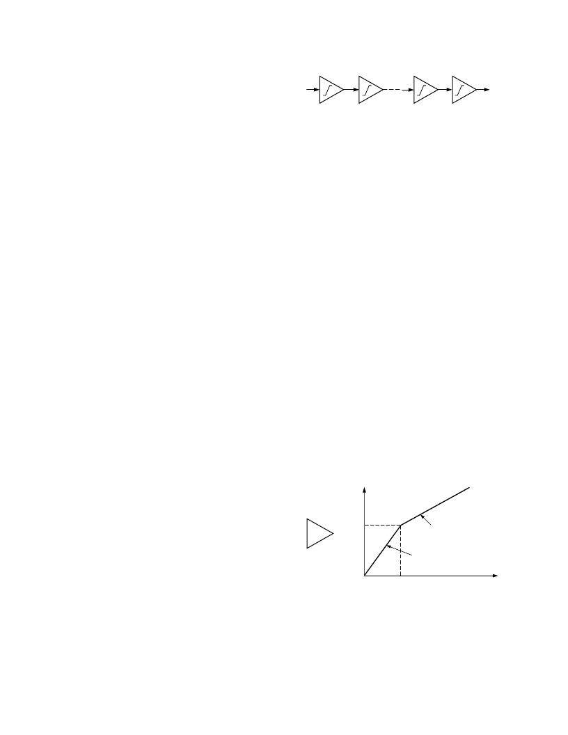
Progressive Compression
High speed, high dynamic range log amps use a cascade of
nonlinear amplifier cells (Figure 20) to generate the logarithmic
function from a series of contiguous segments, a type of piece-
wise-linear technique. This basic topology offers enormous gain-
bandwidth products. For example, the AD8309 employs in its
main signal path six cells each having a small-signal gain of
12.04 dB (
×
4) and a –3 dB bandwidth of 850 MHz, followed by
a final limiter stage whose gain is typically 18 dB. The overall
gain is thus 100,000 (100 dB) and the bandwidth to –10 dB
point at the limiter output is 525 MHz. This very high gain-
bandwidth product (52,500 GHz) is an essential prerequisite to
accurate operation under small signal conditions and at high
frequencies: Equation (2) reminds us that the incremental gain
decreases rapidly as V
IN
increases. The AD8309 exhibits a loga-
rithmic response over most of the range from the noise floor of
–91 dBV, or 28
μ
V rms, (or –78 dBm/50
) to a breakdown-
limited peak input of 4 V (requiring a balanced drive at the
differential inputs INHI and INLO).
(3)
A
V
X
STAGE 1
STAGE 2
STAGE N –1
STAGE N
V
W
A
A
A
Figure 20. Cascade of Nonlinear Gain Cells
Theory of Logarithmic Amplifiers
To develop the theory, we will first consider a somewhat differ-
ent scheme to that employed in the AD8309, but which is sim-
pler to explain, and mathematically more straightforward to
analyze. This approach is based on a nonlinear amplifier unit,
which we may call an A/1 cell, having the transfer characteristic
shown in Figure 21. We here use lowercase variables to define
the local inputs and outputs of these cells, reserving uppercase
for
external
signals.
The small signal gain
V
OUT
/
V
IN
is A, and is maintained for
inputs up to the knee voltage E
K
, above which the
incremental
gain drops to unity. The function is symmetrical: the same drop
in gain occurs for instantaneous values of V
IN
less than –E
K
.
The
large signal
gain has a value of A for inputs in the range
–E
K
<
V
IN
< +E
K
, but falls asymptotically toward unity for very
large inputs.
In logarithmic amplifiers based on this simple function, both the
slope voltage and the intercept voltage must be traceable to the
one reference voltage, E
K
. Therefore, in this fundamental analy-
sis, the
calibration accuracy
of the log amp is dependent solely on
this voltage. In practice, it is possible to separate the basic refer-
ences used to determine V
Y
and V
X
. In the AD8309, V
Y
is trace-
able to an on-chip band-gap reference, while V
X
is derived from
the thermal voltage kT/q and later temperature-corrected by a
precise means.
Let the input of an N-cell cascade be V
IN
, and the final output
V
OUT
. For small signals, the overall gain is simply A
N
. A six-
stage system in which A = 5 (14 dB) has an overall gain of
15,625 (84 dB). The importance of a very high small-signal ac
gain in implementing the logarithmic function has already been
noted. However, this is a parameter of only incidental interest in
the design of log amps; greater emphasis needs to be placed on
the
nonlinear
behavior.
SLOPE = A
SLOPE = 1
OAE
K
0
E
K
INPUT
A/1
Figure 21. The A/1 Amplifier Function
Thus, rather than considering
gain
, we will analyze the overall
nonlinear behavior of the cascade in response to a simple dc
input, corresponding to the V
IN
of Equation (1). For very small
inputs, the output from the first cell is V
1
= AV
IN
; from the
second, V
2
= A
2
V
IN
, and so on, up to V
N
= A
N
V
IN
. At a certain
value of V
IN
, the input to the Nth cell, V
N–1
, is exactly equal to
the knee voltage E
K
. Thus, V
OUT
= AE
K
and since there are N–1
cells of gain A ahead of this node, we can calculate that V
IN
=
E
K
/A
N–1
. This unique point corresponds to the
lin-log transition
,
相關(guān)PDF資料 |
PDF描述 |
|---|---|
| AD830 | High Speed, Video Difference Amplifier(高速,視頻差分運(yùn)放) |
| AD8313ARM-REEL7 | 0.1 GHz-2.5 GHz, 70 dB Logarithmic Detector/Controller |
| AD8313ARM | 0.1 GHz-2.5 GHz, 70 dB Logarithmic Detector/Controller |
| AD8313ARM-REEL | 0.1 GHz-2.5 GHz, 70 dB Logarithmic Detector/Controller |
| AD8313-EVAL | 0.1 GHz-2.5 GHz, 70 dB Logarithmic Detector/Controller |
相關(guān)代理商/技術(shù)參數(shù) |
參數(shù)描述 |
|---|---|
| AD8309ARUZ | 功能描述:IC LOGARITHM AMP 100DB 16-TSSOP RoHS:是 類別:集成電路 (IC) >> 線性 - 放大器 - 專用 系列:- 產(chǎn)品培訓(xùn)模塊:Lead (SnPb) Finish for COTS Obsolescence Mitigation Program 標(biāo)準(zhǔn)包裝:60 系列:- 類型:可變?cè)鲆娣糯笃?應(yīng)用:CATV 安裝類型:表面貼裝 封裝/外殼:20-WQFN 裸露焊盤 供應(yīng)商設(shè)備封裝:20-TQFN-EP(5x5) 包裝:托盤 |
| AD8309ARUZ | 制造商:Analog Devices 功能描述:IC LOGARITHMIC AMP 67NS TSSOP-16 |
| AD8309ARUZ-REEL7 | 功能描述:IC AMP LOG DEMODULATING 16TSSOP RoHS:是 類別:集成電路 (IC) >> 線性 - 放大器 - 專用 系列:- 產(chǎn)品培訓(xùn)模塊:Lead (SnPb) Finish for COTS Obsolescence Mitigation Program 標(biāo)準(zhǔn)包裝:60 系列:- 類型:可變?cè)鲆娣糯笃?應(yīng)用:CATV 安裝類型:表面貼裝 封裝/外殼:20-WQFN 裸露焊盤 供應(yīng)商設(shè)備封裝:20-TQFN-EP(5x5) 包裝:托盤 |
| AD8309-EVAL | 制造商:Analog Devices 功能描述:AD8309 EVALUATION BOARD - Bulk |
| AD8309-EVALZ | 制造商:Analog Devices 功能描述:EVAL KIT FOR 5 MHZ-500 MHZ 100DB DEMODULATING LOGARITHMIC AM - Bulk 制造商:Analog Devices 功能描述:EVAL BOARD, AD8309 LOGARITHMIC AMPLIFIER, Silicon Manufacturer:Analog Devices, Silicon Core Number:AD8309, Kit Application Type:RF / IF, Kit Contents:Eval Board AD8309, Features:(Not Applicable) |
發(fā)布緊急采購(gòu),3分鐘左右您將得到回復(fù)。