- 您現(xiàn)在的位置:買賣IC網(wǎng) > PDF目錄373944 > AD8332ACP-REEL (ANALOG DEVICES INC) Ultralow Noise VGAs with Preamplifier and Programmable RIN PDF資料下載
參數(shù)資料
| 型號(hào): | AD8332ACP-REEL |
| 廠商: | ANALOG DEVICES INC |
| 元件分類: | 消費(fèi)家電 |
| 英文描述: | Ultralow Noise VGAs with Preamplifier and Programmable RIN |
| 中文描述: | SPECIALTY CONSUMER CIRCUIT, QCC32 |
| 封裝: | 5 X 5 MM, MO-220VHHD-2, LFCSP-32 |
| 文件頁(yè)數(shù): | 21/32頁(yè) |
| 文件大小: | 482K |
| 代理商: | AD8332ACP-REEL |
第1頁(yè)第2頁(yè)第3頁(yè)第4頁(yè)第5頁(yè)第6頁(yè)第7頁(yè)第8頁(yè)第9頁(yè)第10頁(yè)第11頁(yè)第12頁(yè)第13頁(yè)第14頁(yè)第15頁(yè)第16頁(yè)第17頁(yè)第18頁(yè)第19頁(yè)第20頁(yè)當(dāng)前第21頁(yè)第22頁(yè)第23頁(yè)第24頁(yè)第25頁(yè)第26頁(yè)第27頁(yè)第28頁(yè)第29頁(yè)第30頁(yè)第31頁(yè)第32頁(yè)
AD8331/AD8332
Gain control noise is a concern in very low noise applications.
Thermal noise in the gain control interface can modulate the
channel gain. The resultant noise is proportional to the output
signal level and usually only evident when a large signal is
present. Its effect is observable only in LO gain mode, where the
noise floor is substantially lower. The gain interface includes an
on-chip noise filter, which reduces this effect significantly at
frequencies above 5 MHz. Care should be taken to minimize
noise impinging at the GAIN input. An external RC filter may
be used to remove V
GAIN
source noise. The filter bandwidth
should be sufficient to accommodate the desired control
bandwidth.
Common-Mode Biasing
An internal bias network connected to a midsupply voltage
establishes common-mode voltages in the VGA and postamp.
An externally bypassed buffer maintains the voltage. The bypass
capacitors form an important ac ground connection, since the
VCM network makes a number of important connections
internally, including the center tap of the VGA’s differential
input attenuator, the feedback network of the VGA’s fixed gain
amplifier, and the feedback network of the postamplifier in both
gain settings. For best results, use a 1 nF and a 0.1 μF capacitor
in parallel, with the 1 nF nearest to Pin VCM. Separate VCM
pins are provided for each channel. For dc-coupling to a 3 V
ADC, the output common-mode voltage is adjusted to 1.5 V by
biasing the VCM pin.
Rev. C | Page 21 of 32
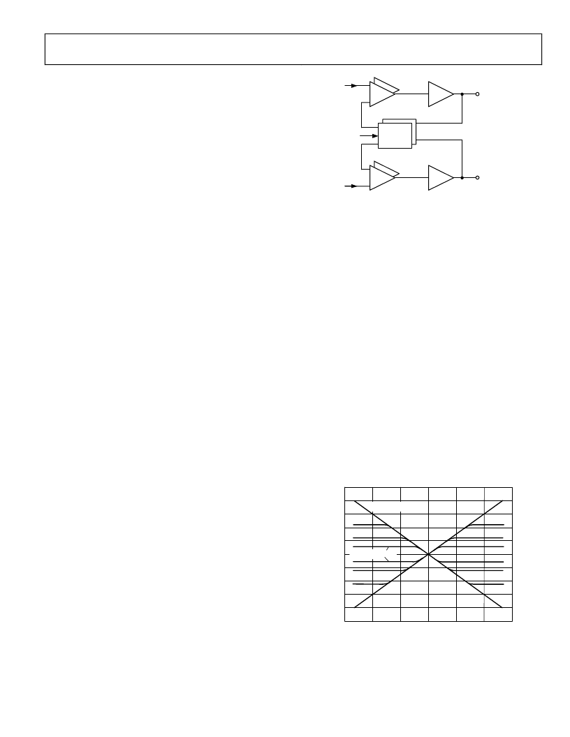
POSTAMPLIFIER
The final stage has a selectable gain of 3.5 dB or 15.5 dB, set by
the logic Pin HILO. These correspond to linear gains of 1.5 or 6.
A simplified block diagram of the postamplifier is shown in
Figure 64.
Separate feedback attenuators implement the two gain settings.
These are selected in conjunction with an appropriately scaled
input stage to maintain a constant 3 dB bandwidth between the
two gain modes (~150 MHz). The slew rate is 1200 V/μs in HI
gain mode and 300 V/μs in LO gain mode. The feedback
networks for HI and LO gain modes are factory trimmed to
adjust the absolute gains of each channel.
Noise
The topology of the postamplifier provides constant input-
referred noise with the two gain settings and variable output-
referred noise. The output-referred noise in HI gain mode
increases (with gain) by four. This setting is recommended
when driving converters with higher noise floors. The extra gain
boosts the output signal levels and noise floor appropriately.
When driving circuits with lower input noise floors, the LO gain
mode optimizes the output dynamic range.
Gm2
+
–
Gm1
VOH
VOL
VCM
Gm1
Gm2
F1
F2
0
Figure 64. Postamplifier Block Diagram
Although the quantization noise floor of an ADC depends on a
number of factors, the 48 nV/√Hz and 178 nV/√Hz levels are
well suited to the average requirements of most 12-bit and
10-bit converters, respectively. An additional technique,
described in the Applications section, can extend the noise floor
even lower for possible use with 14-bit ADCs.
Output Clamping
Outputs are internally limited to a level of 4.5 V p-p differential
when operating at a 2.5 V common-mode voltage. The postamp
implements an optional output clamp engaged through a
resistor from R
CLMP
to ground. Table shows a list of
recommended resistor values.
Output clamping can be used for ADC input overload
protection, if needed, or postamp overload protection when
operating from a lower common-mode level, such as 1.5 V. The
user should be aware that distortion products increase as output
levels approach the clamping levels and should adjust the clamp
resistor accordingly. Also, see the Applications section.
The accuracy of the clamping levels is approximately ±5% in LO
or HI mode. Figure 65 illustrates the output characteristics for a
few values of R
CLMP
.
–3
–2
V
INH
(V)
V
O
,
O
0
–1
0.5
2
1
3
1.0
4.5
4.0
3.5
3.0
2.5
2.0
1.5
0
5.0
8.8k
3.5k
R
CLMP
=
∞
R
CLMP
= 1.86k
0
Figure 65. Output Clamping Characteristics
相關(guān)PDF資料 |
PDF描述 |
|---|---|
| AD8332ACP-REEL7 | Ultralow Noise VGAs with Preamplifier and Programmable RIN |
| AD8332ARU | Ultralow Noise VGAs with Preamplifier and Programmable RIN |
| AD8331ARQ-REEL | Ultralow Noise VGAs with Preamplifier and Programmable RIN |
| AD8331ARQ-REEL7 | Ultralow Noise VGAs with Preamplifier and Programmable RIN |
| AD8341 | 1.5 GHz to 2.4 GHz RF Vector Modulator |
相關(guān)代理商/技術(shù)參數(shù) |
參數(shù)描述 |
|---|---|
| AD8332ACP-REEL7 | 制造商:Analog Devices 功能描述:SP Amp Variable Gain Amp Dual 5.5V 32-Pin LFCSP EP T/R 制造商:Rochester Electronics LLC 功能描述: |
| AD8332ACPZ-R2 | 功能描述:IC AMP VGA PREAMP PROGR 32-LFCSP RoHS:是 類別:集成電路 (IC) >> 線性 - 放大器 - 專用 系列:X-AMP® 產(chǎn)品培訓(xùn)模塊:Lead (SnPb) Finish for COTS Obsolescence Mitigation Program 標(biāo)準(zhǔn)包裝:60 系列:- 類型:可變?cè)鲆娣糯笃?應(yīng)用:CATV 安裝類型:表面貼裝 封裝/外殼:20-WQFN 裸露焊盤 供應(yīng)商設(shè)備封裝:20-TQFN-EP(5x5) 包裝:托盤 |
| AD8332ACPZ-R7 | 功能描述:IC AMP VAR GAIN 2CHAN 32-LFCSP RoHS:是 類別:集成電路 (IC) >> 線性 - 放大器 - 專用 系列:X-AMP® 產(chǎn)品培訓(xùn)模塊:Lead (SnPb) Finish for COTS Obsolescence Mitigation Program 標(biāo)準(zhǔn)包裝:60 系列:- 類型:可變?cè)鲆娣糯笃?應(yīng)用:CATV 安裝類型:表面貼裝 封裝/外殼:20-WQFN 裸露焊盤 供應(yīng)商設(shè)備封裝:20-TQFN-EP(5x5) 包裝:托盤 |
| AD8332ACPZ-RL | 功能描述:IC AMP VAR GAIN 2CHAN 32LFCSP RoHS:是 類別:集成電路 (IC) >> 線性 - 放大器 - 專用 系列:X-AMP® 產(chǎn)品培訓(xùn)模塊:Lead (SnPb) Finish for COTS Obsolescence Mitigation Program 標(biāo)準(zhǔn)包裝:60 系列:- 類型:可變?cè)鲆娣糯笃?應(yīng)用:CATV 安裝類型:表面貼裝 封裝/外殼:20-WQFN 裸露焊盤 供應(yīng)商設(shè)備封裝:20-TQFN-EP(5x5) 包裝:托盤 |
| AD8332ARU | 功能描述:IC VGA DUAL W/PREAMP LN 28-TSSOP RoHS:否 類別:集成電路 (IC) >> 線性 - 放大器 - 專用 系列:X-AMP® 產(chǎn)品培訓(xùn)模塊:Lead (SnPb) Finish for COTS Obsolescence Mitigation Program 標(biāo)準(zhǔn)包裝:60 系列:- 類型:可變?cè)鲆娣糯笃?應(yīng)用:CATV 安裝類型:表面貼裝 封裝/外殼:20-WQFN 裸露焊盤 供應(yīng)商設(shè)備封裝:20-TQFN-EP(5x5) 包裝:托盤 |
發(fā)布緊急采購(gòu),3分鐘左右您將得到回復(fù)。