- 您現(xiàn)在的位置:買(mǎi)賣(mài)IC網(wǎng) > PDF目錄373944 > AD8347-EVAL (Analog Devices, Inc.) 0.8 GHz-2.7 GHz Direct Conversion Quadrature Demodulator PDF資料下載
參數(shù)資料
| 型號(hào): | AD8347-EVAL |
| 廠商: | Analog Devices, Inc. |
| 英文描述: | 0.8 GHz-2.7 GHz Direct Conversion Quadrature Demodulator |
| 中文描述: | 0.8千兆赫- 2.7 GHz直接轉(zhuǎn)換正交解調(diào)器 |
| 文件頁(yè)數(shù): | 17/20頁(yè) |
| 文件大小: | 750K |
| 代理商: | AD8347-EVAL |
第1頁(yè)第2頁(yè)第3頁(yè)第4頁(yè)第5頁(yè)第6頁(yè)第7頁(yè)第8頁(yè)第9頁(yè)第10頁(yè)第11頁(yè)第12頁(yè)第13頁(yè)第14頁(yè)第15頁(yè)第16頁(yè)當(dāng)前第17頁(yè)第18頁(yè)第19頁(yè)第20頁(yè)
REV. 0
AD8347
–17–
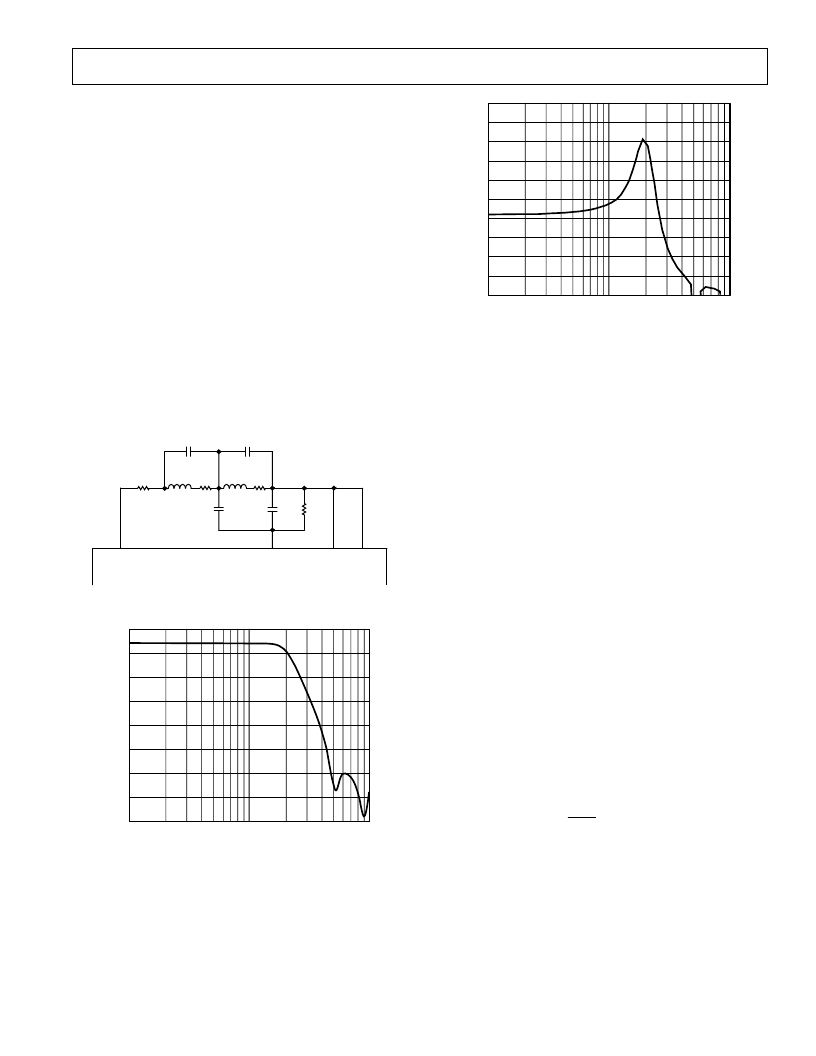
Filter Design Considerations
Baseband low-pass or band-pass filtering can be conveniently
performed between the mixer outputs (IMXO/QMXO) and the
input to the baseband amplifiers. Because the output impedance
of the mixer is low (roughly 3
) and the input impedance of
the baseband amplifier is high, it is not practical to design a
filter which is reactively matched to these impedances. An LC
filter can be matched by placing a series resistor at the mixer
output and a shunt resistor (terminated to V
VREF
) at the input to
the baseband amplifier.
Because the mixer output drive level is limited to a maximum cur-
rent of 1.5 mA, the characteristic impedance of the filter should be
greater than 50
, especially if larger signal swings are to be achieved.
Figure 8 shows the schematic for a 100
, fourth order elliptic
low-pass filter with a 3 dB cutoff frequency of 20 MHz. Source
and load impedances of approximately 100
ensure that the
filter sees a matched source and load. This also ensures that the
mixer output is driving an overall load of 200
. Note that the
shunt termination resistor is tied to VREF and not to ground.
The frequency response and group delay of this filter are shown
in Figures 9 and 10.
IMXO
AD8347
VREF
VDT1
(SEE
TEXT)
L
1.2 H
R3
2
IAIN
R4
2
C1
4.7pF
C3
8.2pF
C2
150pF
RS
95.3
L
0.68 H
C4
82pF
RL
100
Figure 8. Typical Baseband Low-Pass Filter
FREQUENCY
–
MHz
–
80
1
100
10
A
–
–
70
–
60
–
50
–
40
–
30
–
20
–
10
0
Figure 9. Frequency Response of 20 MHz Baseband
Low-Pass Filter
FREQUENCY
–
MHz
0
1
100
10
G
–
5
10
15
20
25
30
35
40
45
50
Figure 10. Group Delay of 20 MHz Baseband Low-Pass
Filter
If the VGA is operating in AGC mode, the detector input (VDT1/
VDT2) can be tied either to the input or output of the filter.
Connecting the detector input to the input of the filter (i.e.,
IMXO and QMXO) will cause the VGA leveling point to be
determined by the composite of the wanted signal and any unfiltered
components such as blockers or signal harmonics. Connecting
VDT1/VDT2 to the
outputs
of the filters ensures that the leveling
point of the AGC circuit is based upon the amplitude of the
filtered output only. The latter option is more desirable as it
results in a more constant baseband output. However, when
using this method, the leveling point of the AGC should be set
so that out-of-band blockers do not overdrive the mixer output.
DC Offset Compensation
Feedthrough of the LO signal to the RF input port results in
self-mixing of the LO signal. This produces a dc component
at the mixer output that is frequency-dependent.
The AD8347 includes an internal circuit which actively nulls
out any dc offsets that appear at the mixer output. The dc-bias
level of the mixer output (which should ideally be equal to V
VREF
,
the bias level for the baseband sections of the chip) is continually
being compared to V
VREF
. Any differences between the mixer
output level and V
VREF
, will force a compensating voltage on to
the mixer output.
The time constant of this correction loop is set by the capacitors
which are connected to pins IOFS and QOFS (each output can
be compensated separately). For normal operation 0.1
μ
F capacitors
are recommended. The corner frequency of the compensation
loop is given approximately by the equation
f
C
C
(
in F
dB
OFS
OFS
3
40
=
)
The corner frequency must be set to a frequency that is much
lower than the symbol rate of the demodulated data. This prevents
the compensation loop from falsely interpreting the data stream
as a changing offset voltage.
To disable the offset compensation circuits, IOFS and QOFS
should be tied to VREF.
相關(guān)PDF資料 |
PDF描述 |
|---|---|
| AD8347ARU | 0.8 GHz-2.7 GHz Direct Conversion Quadrature Demodulator |
| AD8347ARU-REEL7 | 0.8 GHz-2.7 GHz Direct Conversion Quadrature Demodulator |
| AD8348 | 50-1000 MHz Quadrature Demodulator |
| AD8348-EVAL | 50-1000 MHz Quadrature Demodulator |
| AD8348XXX | 50-1000 MHz Quadrature Demodulator |
相關(guān)代理商/技術(shù)參數(shù) |
參數(shù)描述 |
|---|---|
| ad8347-evalz | 制造商:Analog Devices 功能描述:EVAL BD 0.8 GHZ TO 2.7 GHZ DIRECT CONVERSION QUADRATURE DEMO - Bulk |
| AD8348 | 制造商:AD 制造商全稱(chēng):Analog Devices 功能描述:400 MHz to 6 GHz Broadband Quadrature Modulator |
| AD8348ARE | 制造商:Analog Devices 功能描述:QUADRATURE MODULATOR - Rail/Tube |
| AD8348ARU | 功能描述:IC QUADRATUR DEMOD 50MHZ 28TSSOP RoHS:否 類(lèi)別:RF/IF 和 RFID >> RF 解調(diào)器 系列:- 產(chǎn)品培訓(xùn)模塊:Lead (SnPb) Finish for COTS Obsolescence Mitigation Program 標(biāo)準(zhǔn)包裝:2,500 系列:- 功能:解調(diào)器 LO 頻率:- RF 頻率:70MHz ~ 300MHz P1dB:-9dBm 增益:- 噪音數(shù)據(jù):6.36dB 電流 - 電源:41.5mA 電源電壓:2.7 V 封裝/外殼:28-WFQFN 裸露焊盤(pán) 供應(yīng)商設(shè)備封裝:28-TQFN-EP(5x5) 包裝:帶卷 (TR) |
| AD8348ARU-REEL7 | 功能描述:IC QUADRATUR DEMOD 50MHZ 28TSSOP RoHS:否 類(lèi)別:RF/IF 和 RFID >> RF 解調(diào)器 系列:- 產(chǎn)品培訓(xùn)模塊:Lead (SnPb) Finish for COTS Obsolescence Mitigation Program 標(biāo)準(zhǔn)包裝:2,500 系列:- 功能:解調(diào)器 LO 頻率:- RF 頻率:70MHz ~ 300MHz P1dB:-9dBm 增益:- 噪音數(shù)據(jù):6.36dB 電流 - 電源:41.5mA 電源電壓:2.7 V 封裝/外殼:28-WFQFN 裸露焊盤(pán) 供應(yīng)商設(shè)備封裝:28-TQFN-EP(5x5) 包裝:帶卷 (TR) |
發(fā)布緊急采購(gòu),3分鐘左右您將得到回復(fù)。